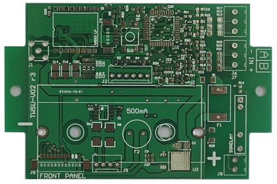
 PCB
PCB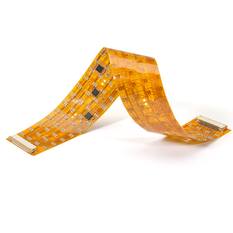 FPC
FPC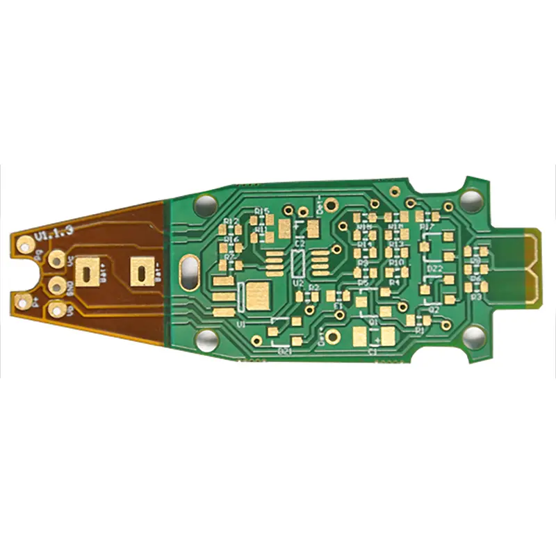 Rigid-Flex
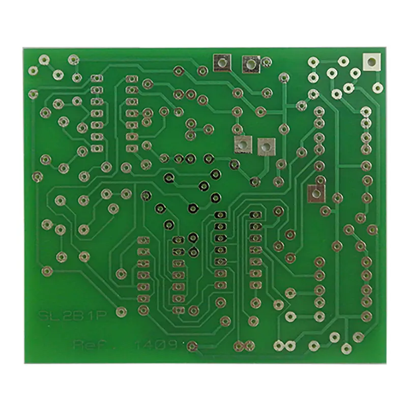 FR-4
FR-4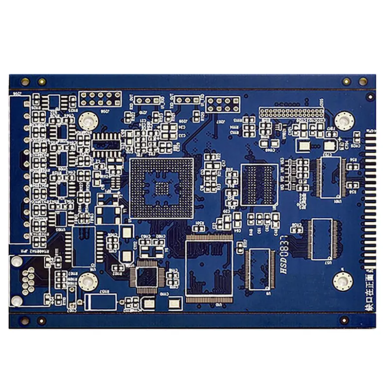 HDI PCB
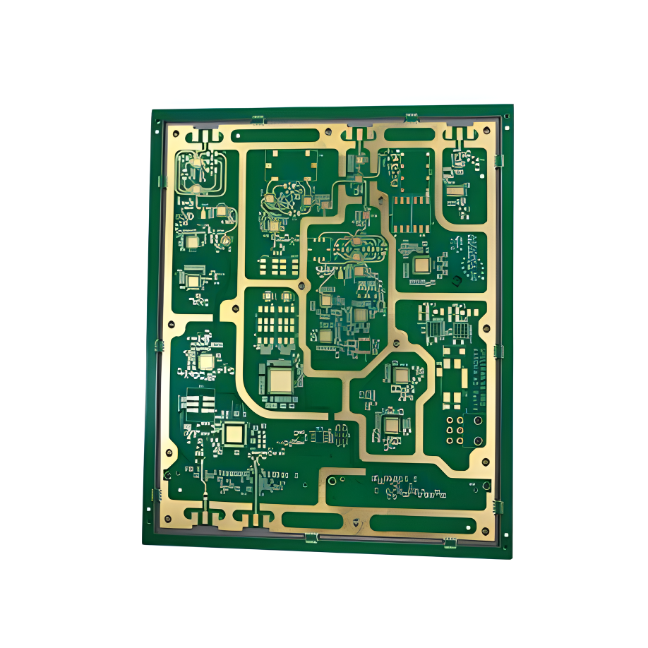 Rogers High-Frequency Board
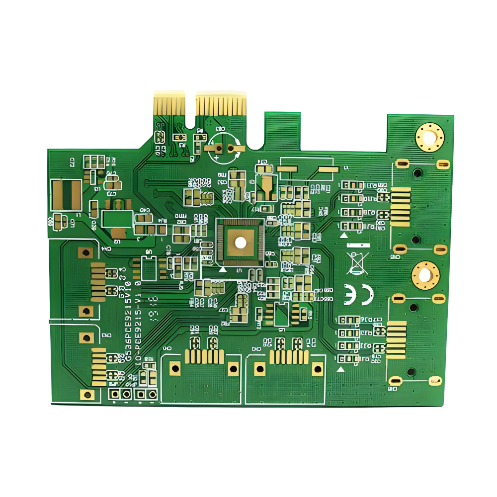 PTFE Teflon High-Frequency Board
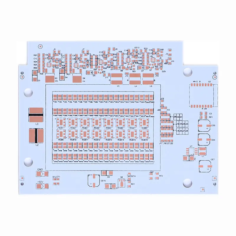 Aluminum
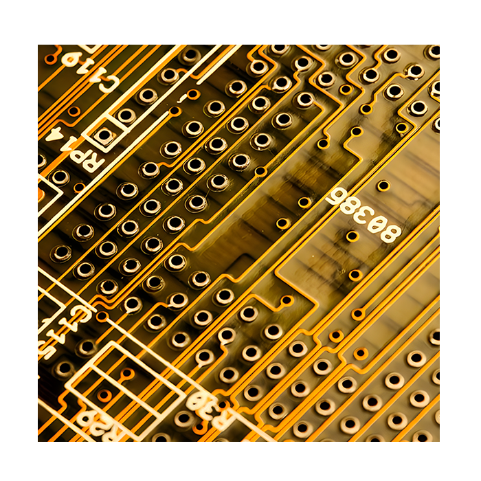 Copper Core
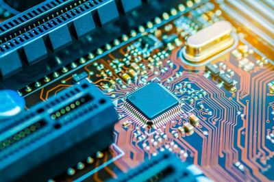 PCB Assembly
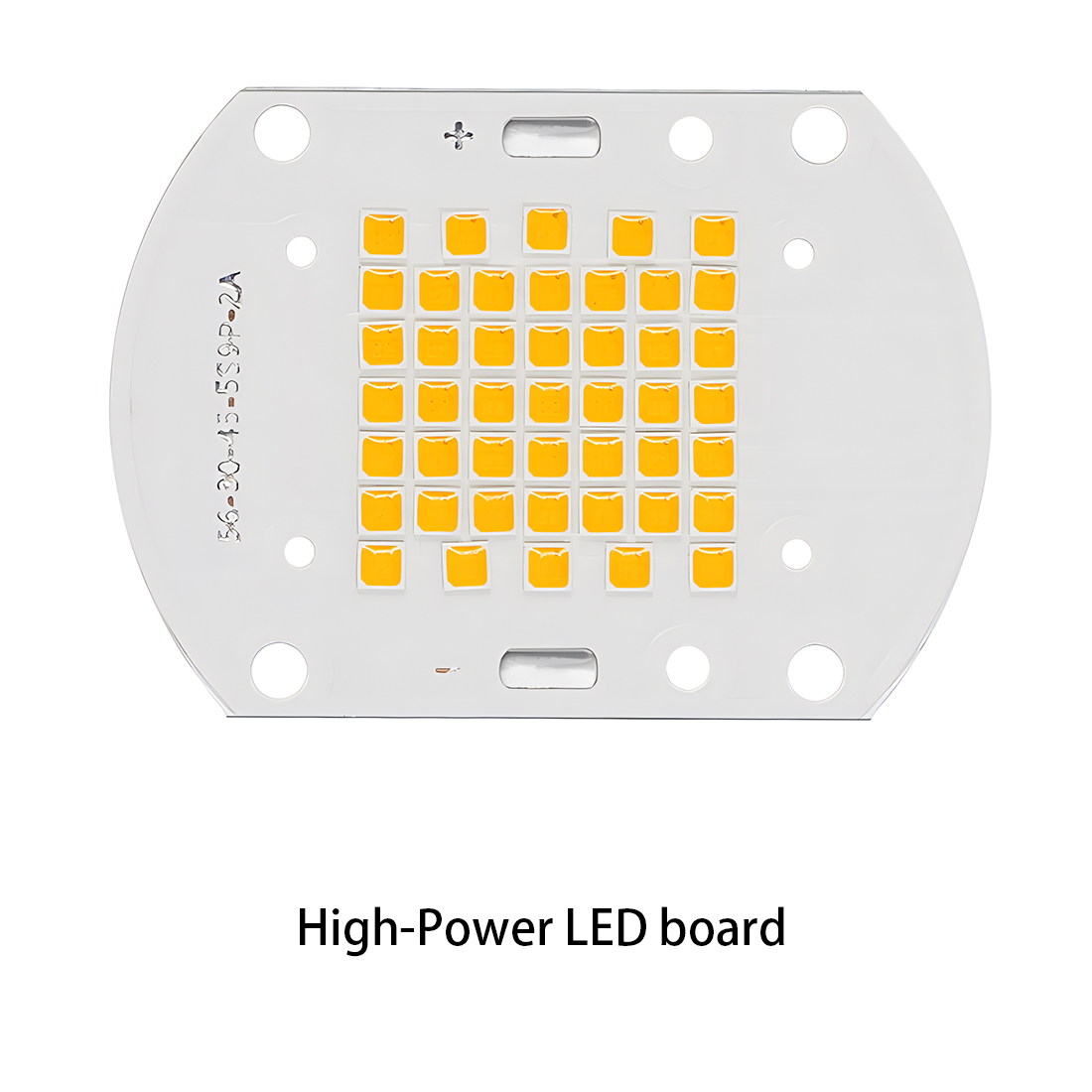 LED light PCBA
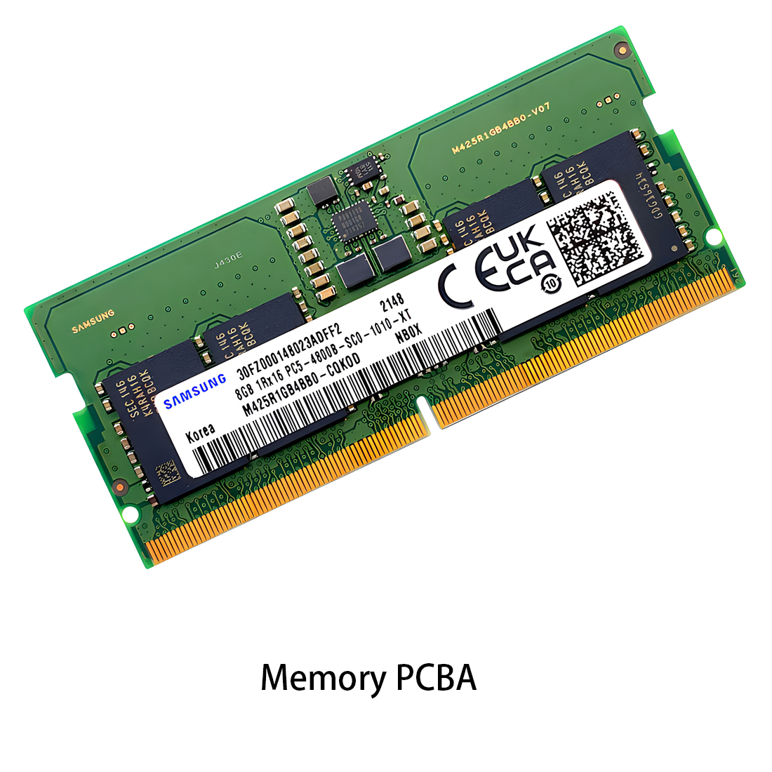 Memory PCBA
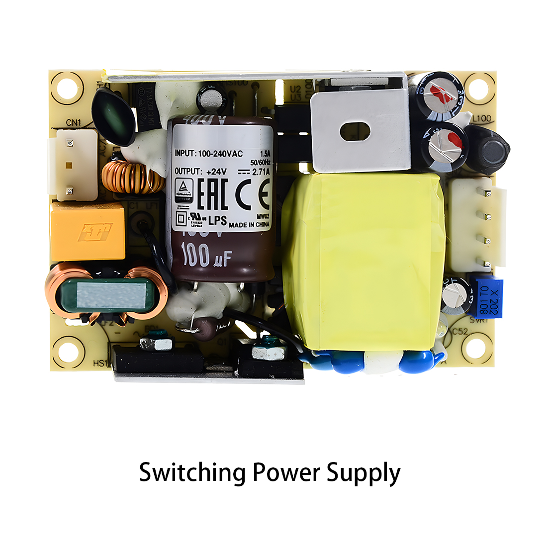 Power Supply PCBA
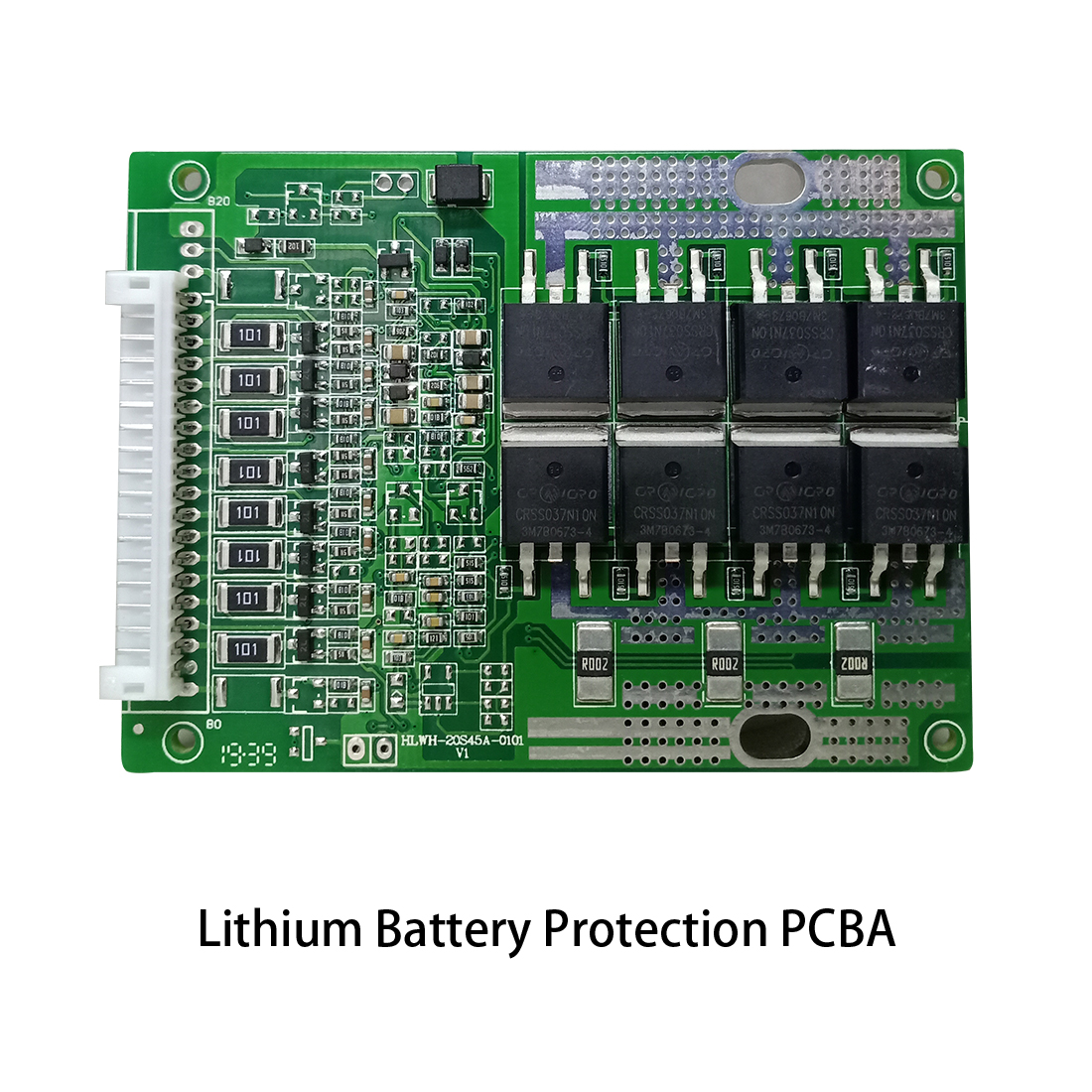 New Energey PCBA
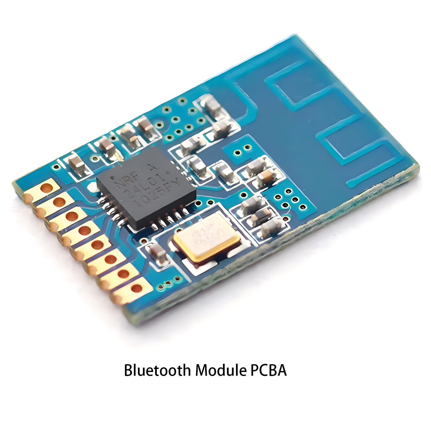 Communication PCBA
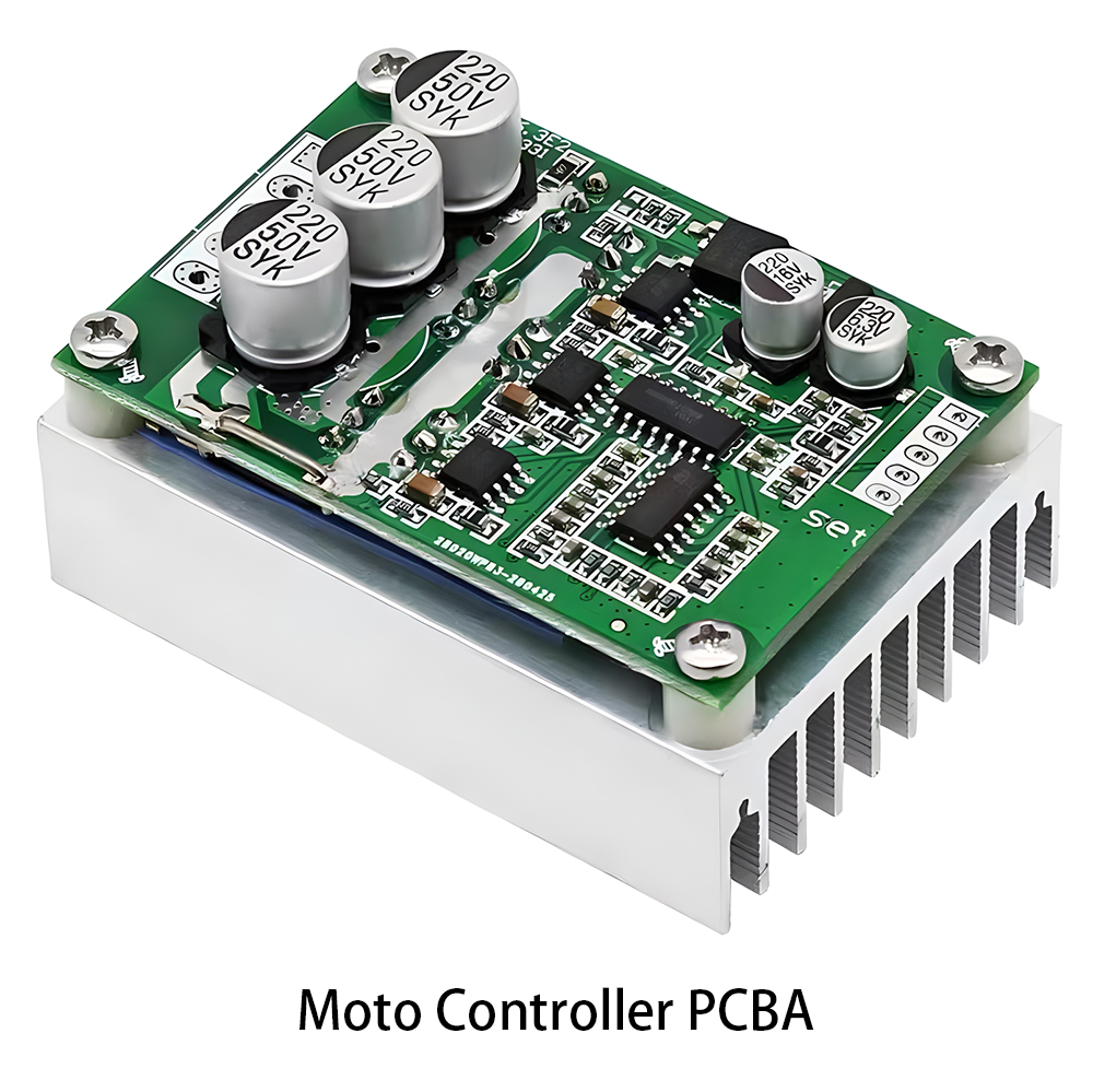 Industrial Control PCBA
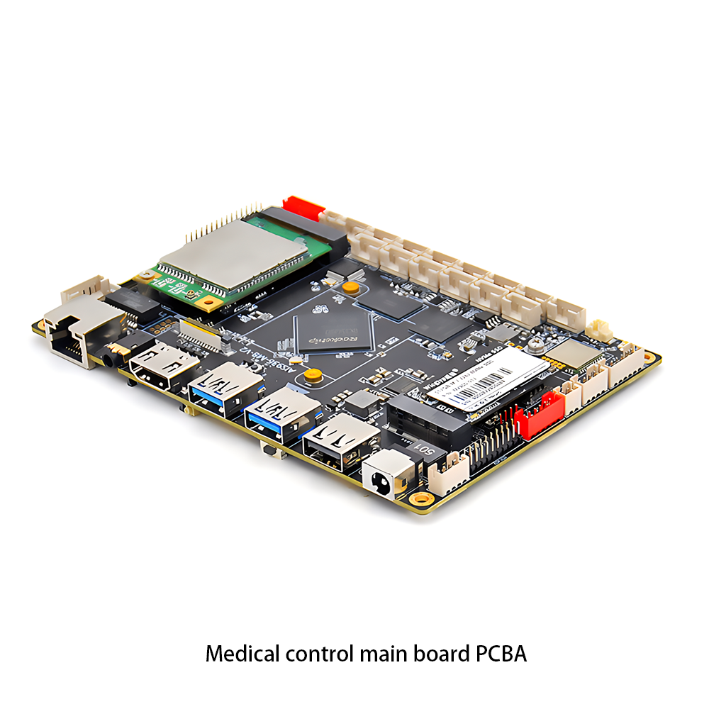 Medical Equipment PCBA
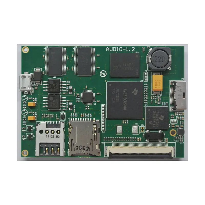 Testing Service
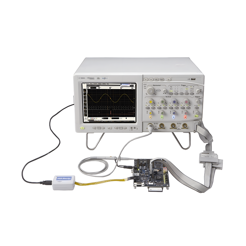 PCBA Testing Service
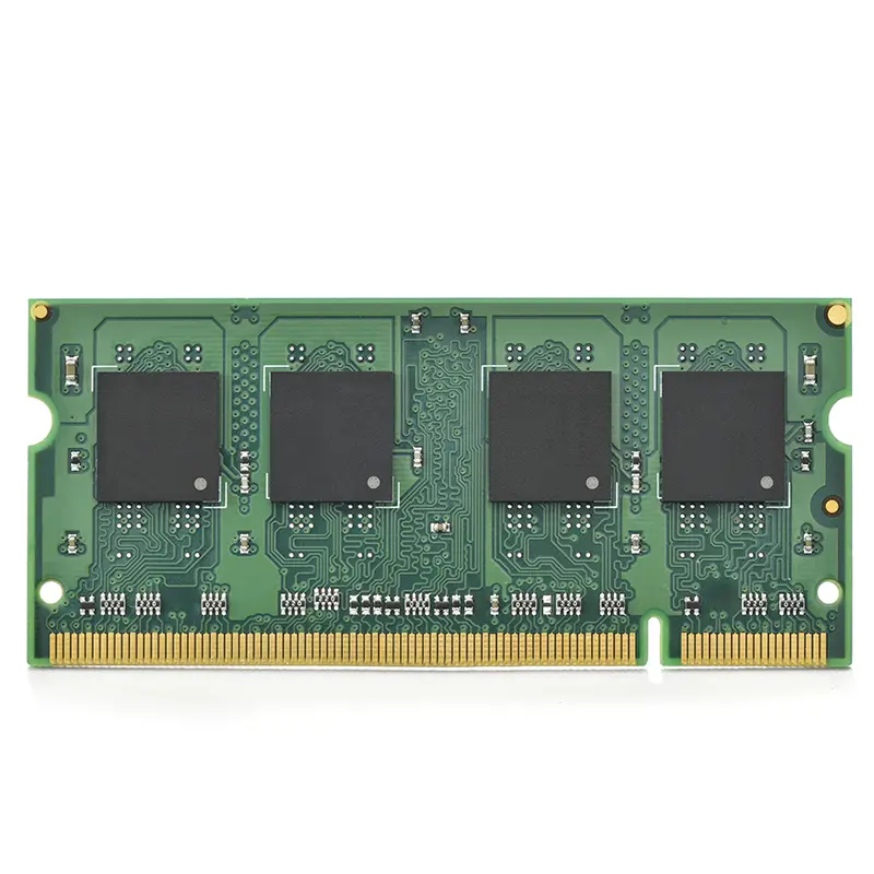 Certification Application
 RoHS Certification Application
 REACH Certification Application
 CE Certification Application
 FCC Certification Application
 CQC Certification Application
 UL Certification Application
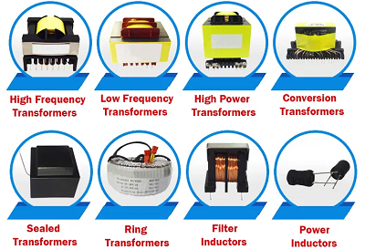 Transformers, Inductors
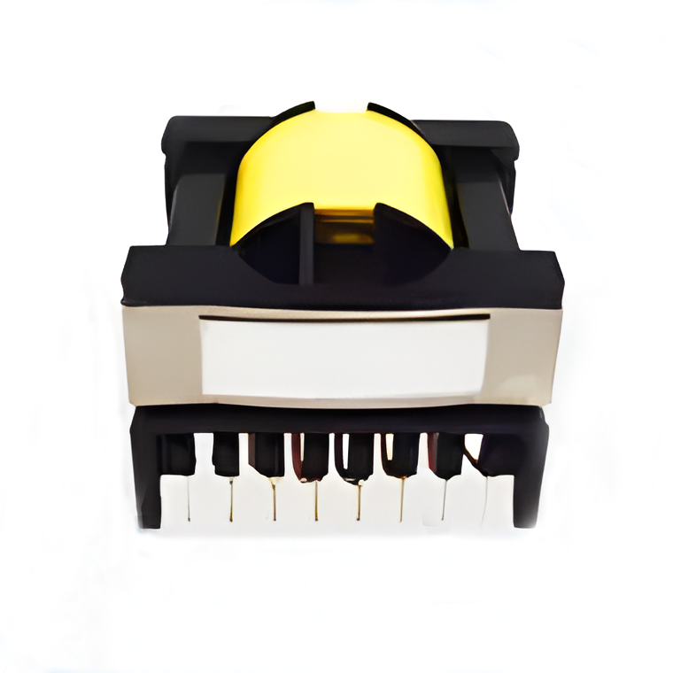 High Frequency Transformers
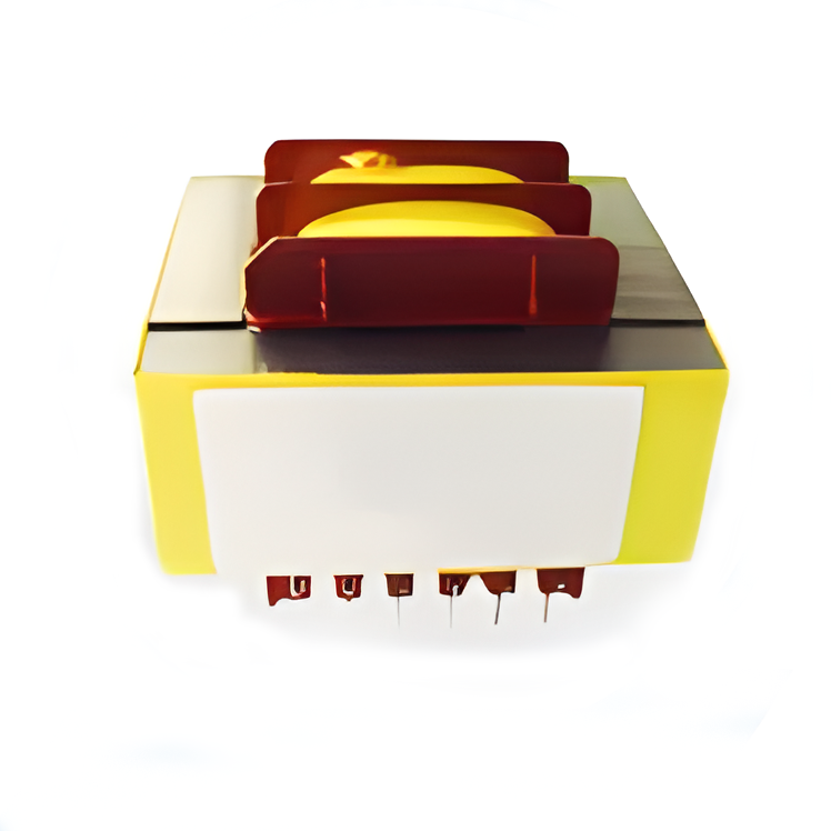 Low Frequency Transformers
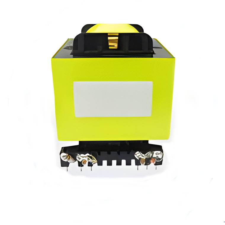 High Power Transformers
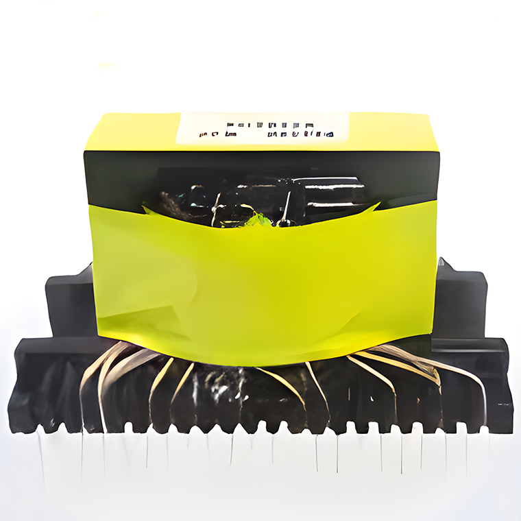 Conversion Transformers
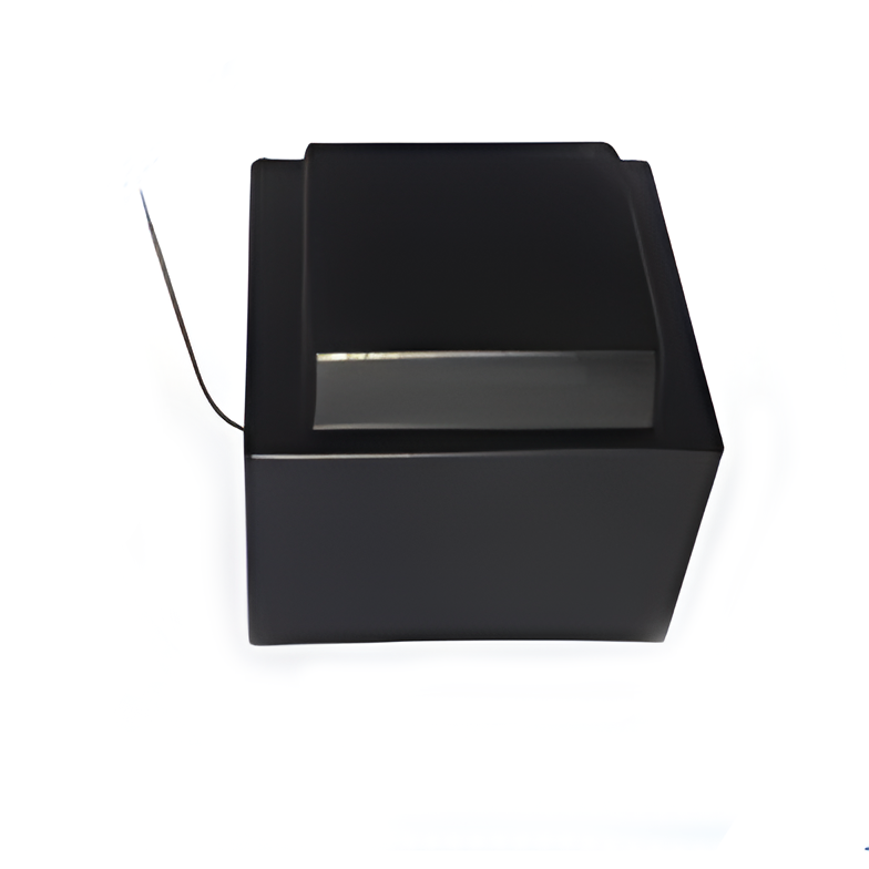 Sealed Transformers
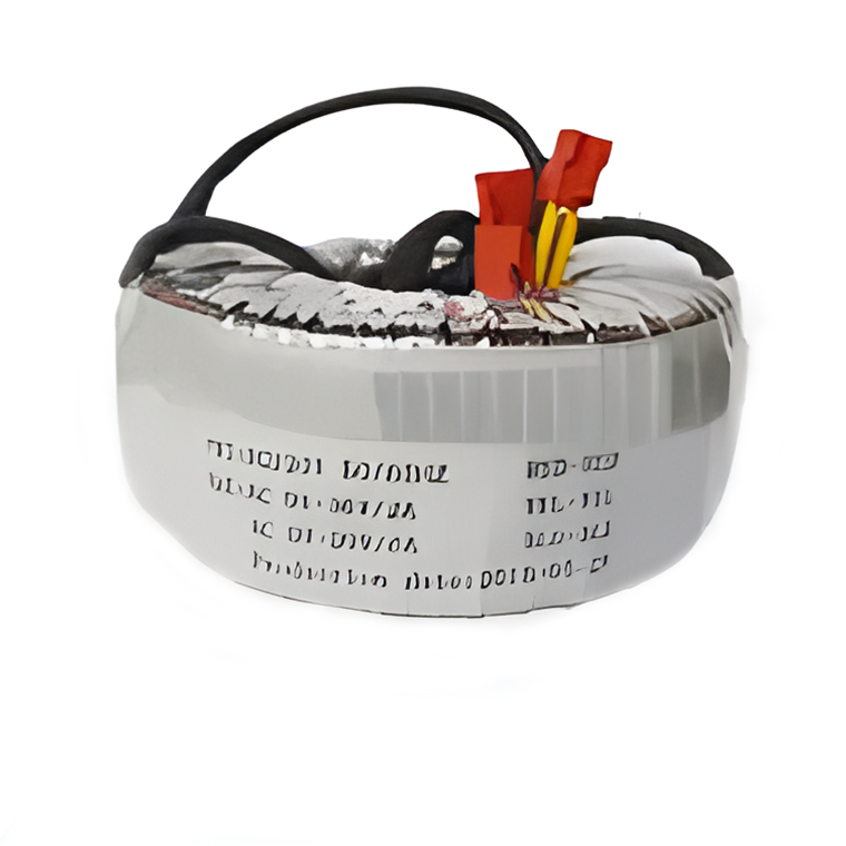 Ring Transformers
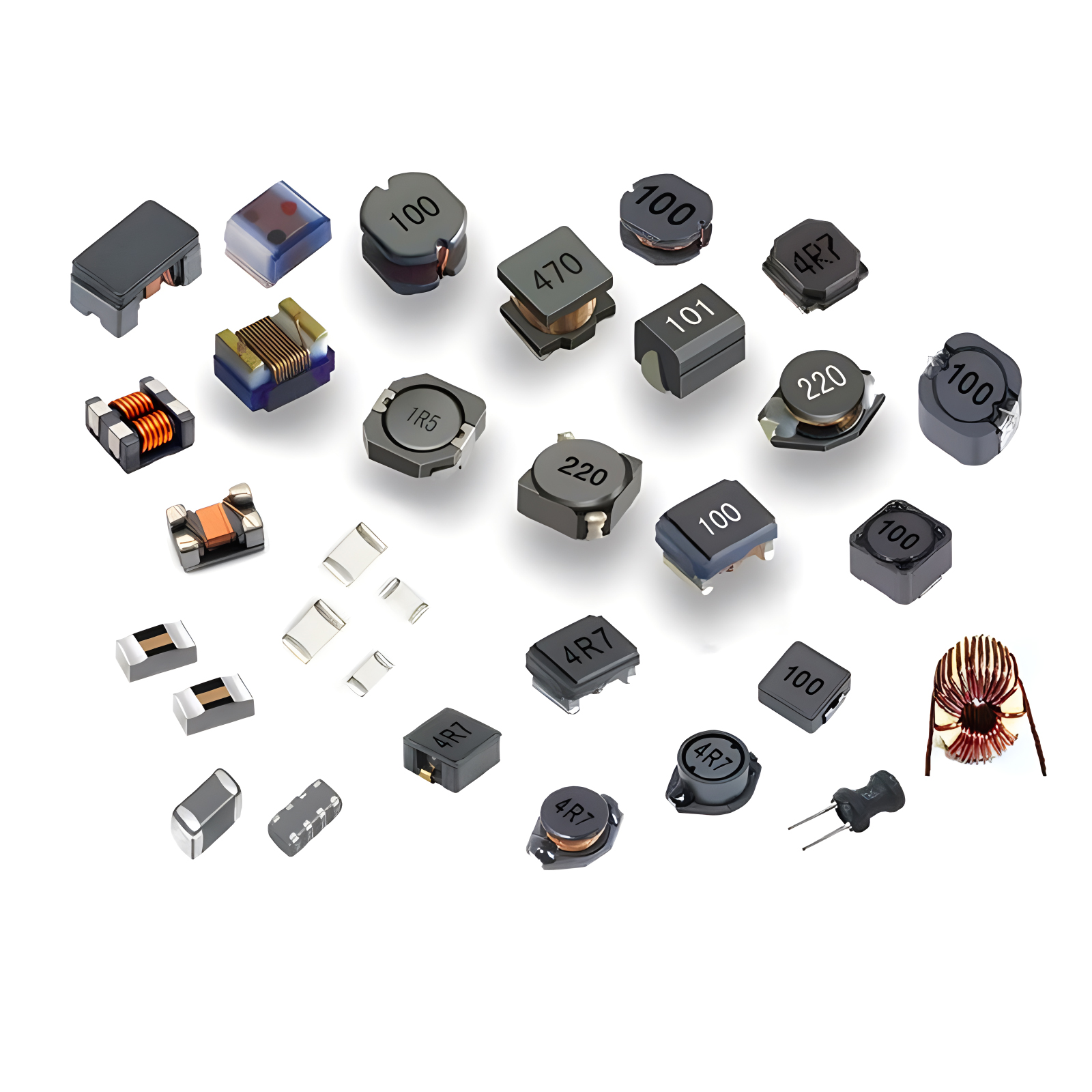 Inductors
 Wires,Cables Customized
 Network Cables
 Power Cords
 Antenna Cables
 Coaxial Cables
 Net Position Indicator(网位仪)
 Capacitors
 Connectors
 Diodes
 Embedded Processors & Controllers
 Digital Signal Processors (DSP/DSC)
 Microcontrollers (MCU/MPU/SOC)
 Programmable Logic Device(CPLD/FPGA)
 Communication Modules/IoT
 Resistors
 Through Hole Resistors
 Resistor Networks, Arrays
 Potentiometers,Variable Resistors
 Aluminum Case,Porcelain Tube Resistance
 Current Sense Resistors,Shunt Resistors
 Switches
 Transistors
 Power Modules
 Isolated Power Modules
 AC-DC Power Modules
 DC-AC Module(Inverter)
 RF and Wireless
R&D
Minintel operates a research and development center in Shenzhen, where it has accumulated over 15 years of experience in relevant product development. This wealth of experience has fostered a mature product development capability, enabling us to offer clients a complete set of solutions ranging from conceptual design to mass production.


Professional Project Management Team
In the New Product Introduction (NPI) phase, a professional Project Management Team fulfills and realizes customer needs in the following 7 areas:


DFA (Design for Assembly)
When designing products, consider the convenience of assembly and manufacturing, offering suggestions to simplify assembly components, shorten the required assembly time, and reduce assembly costs.
Analysis of Design Simplification
Rationality Analysis of Part Distribution
Robustness Analysis of Products
Structural Analysis of Parts and Components
Rationality Analysis of Assembly Process


DFM(Design for Manufacture)
DFM is a methodology that, during the design phase, takes into consideration the manufacturing process, design characteristics, material selection, environmental factors, and testing requirements. Its aim is to identify and analyze potential risks, provide improvement suggestions, and ensure the manufacturability and production efficiency of the product.
PCB Board Design Analysis
Assembly Analysis
Panelization Analysis
Microvia Analysis
Structural Component Design Analysis


DFR(Design for Reliability)
DFR is a systematic approach aimed at eliminating potential flaws and weak points in products by establishing reliability models, conducting reliability analysis and validation, evaluating and optimizing designs, thereby reducing product risk.
Product Reliability Design and Validation
PCBA Process Reliability Analysis and Evaluation
EMC (Electromagnetic Compatibility) Design and Remediation


DFT(Design for Test)
DFT is a design philosophy that incorporates testability features into the design of electronic products to facilitate efficient and effective testing. By doing so, it aims to enhance product quality while reducing testing costs. Key elements of DFT include:
Development of ICT (In-Circuit Test), FCT (Functional Circuit Test), and Flying Probe Test Strategies: These tests are designed to verify the functionality of individual components and the entire circuit board respectively. ICT checks for component presence, value, and solder joint integrity; FCT simulates the operational environment to test circuit functionality; and Flying Probe tests offer flexibility in testing complex boards without the need for a fixture.
AOI (Automated Optical Inspection) and X-ray Testing Solutions:AOI systems use cameras and optical sensors to inspect the surface of printed circuit boards for defects such as missing or damaged components, incorrect component placement, and solder defects. X-ray testing is particularly useful for inspecting internal structures of components and solder joints that are not visible from the surface, ensuring integrity even in densely populated or multi-layer boards.


Hardware Design
This involves the conceptualization and creation of physical electronic devices or systems. It includes selecting appropriate components, defining their functional and performance specifications, and designing how they work together to achieve the desired functionality.
RF (Radio Frequency) Design
Platform Design
PCB (Printed Circuit Board) Design
Reliability Design

