

Copper PCB
A Copper PCB, or Copper-Based Printed Circuit Board, is the most common type of printed circuit board used in electronics. The term "Copper PCB" generally refers to a PCB that uses copper as the primary conductive material for its circuitry. Copper is widely used due to its excellent electrical conductivity, ductility, and relatively low cost.
In a Copper PCB, thin layers of copper are laminated onto one or both sides of a non-conductive substrate, usually made of materials like FR-4 (a glass-fiber reinforced epoxy laminate), CEM-1 (a paper and epoxy resin material), or polytetrafluoroethylene (PTFE, commonly known as Teflon). The copper layers are then patterned using photolithography and etching processes to create the desired circuit paths, connecting various electronic components such as resistors, capacitors, and integrated circuits.
| No. | Item | Process Capability Parameter |
|---|---|---|
| 1 | Base Material | Copper Core |
| 2 | Number of Layers | 1 Layer, 2 Layers, 4 Layers |
| 3 | PCB Size | Minimum Size: 5*5mm
Maximum Size: 480*286mm
|
| 4 | Quality Grade | Standard IPC 2,IPC 3 |
| 5 | Thermal Conductivity (W/m*K) | 380W |
| 6 | Board Thickness | 1.0mm~2.0mm |
| 7 | Min Tracing/Spacing | 4mil / 4mil |
| 8 | Plated Through-hole size | ≥0.2mm |
| 9 | Non-Plated Through-hole size | ≥0.8mm |
| 10 | Copper Thickness | 1oz, 2oz, 3oz, 4oz, 5oz |
| 11 | Solder Mask | Green, Red, Yellow, White, Black, Blue, Purple, Matte Green, Matte Black, None |
| 12 | Surface Finish | Immersion Gold, OSP, Hard Gold, ENEPIG, Immersion Silver, None |
| 13 | Other Options | Countersinks, Castellated Holes, Custom Stackup and so on. |
| 14 | Certification | ISO9001, UL, RoHS, REACH |
| 15 | Testing | AOI, SPI, X-ray, Flying Probe |

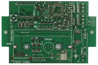 PCB
PCB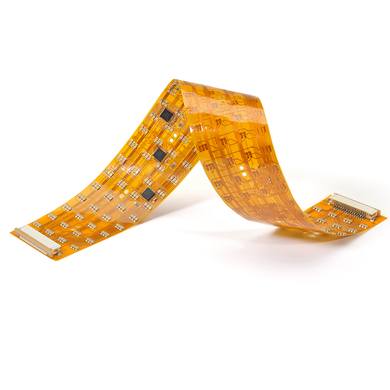 FPC
FPC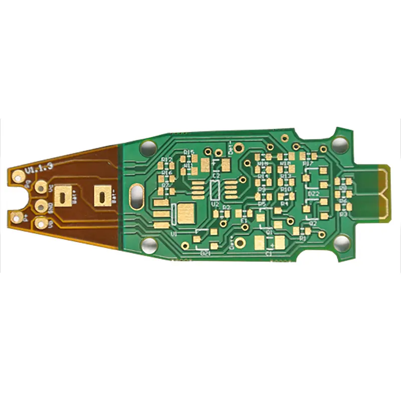 Rigid-Flex
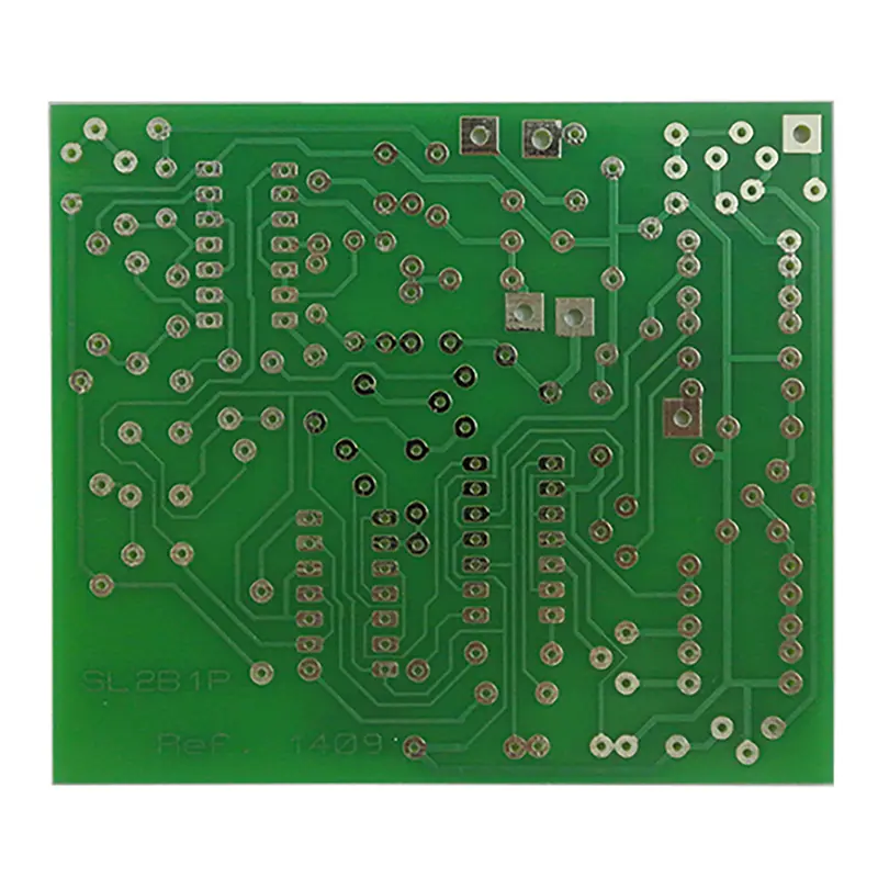 FR-4
FR-4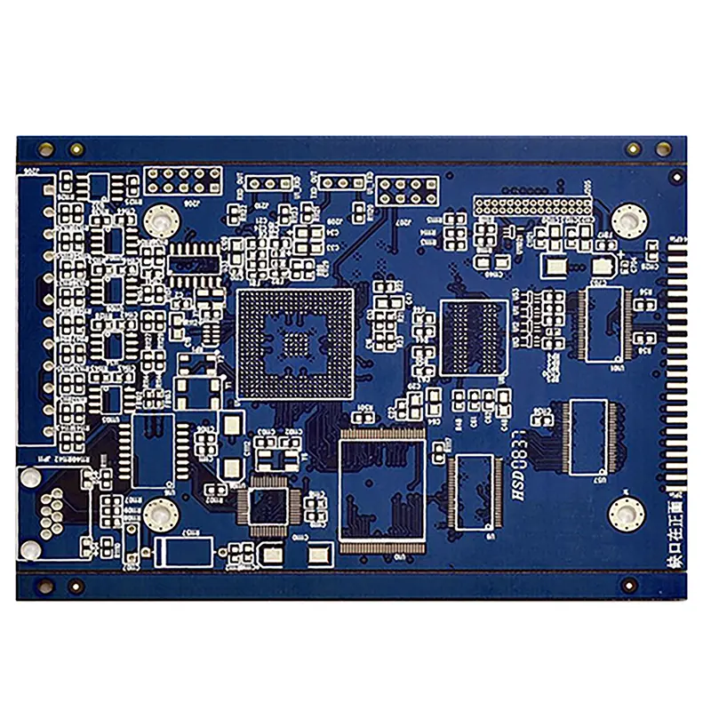 HDI PCB
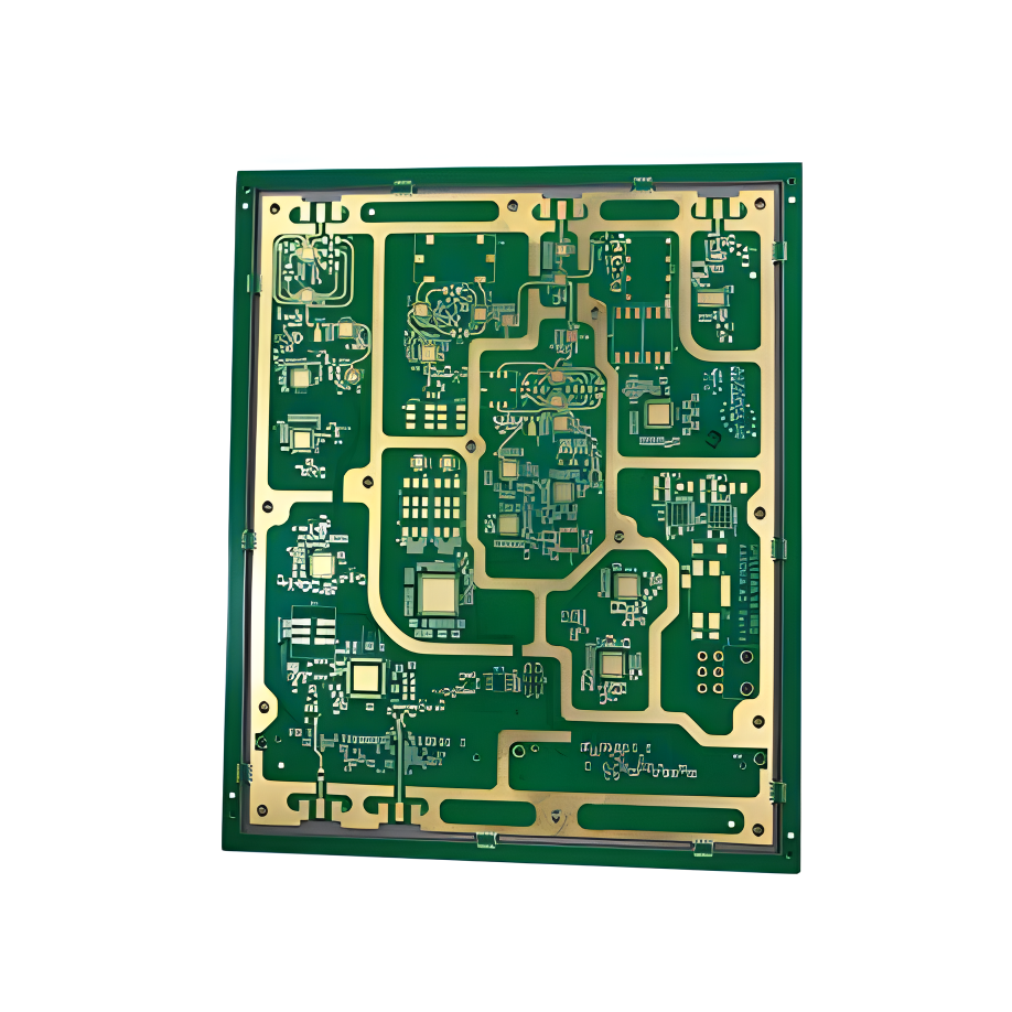 Rogers High-Frequency Board
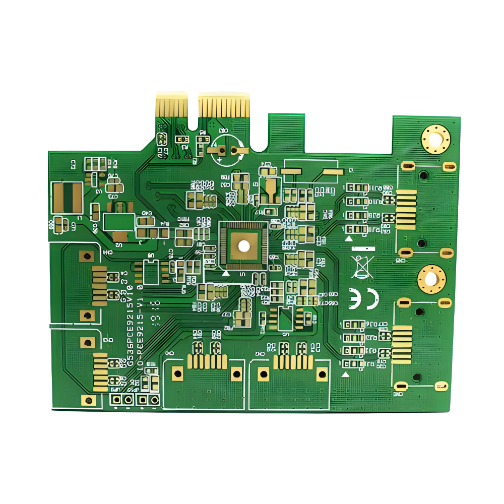 PTFE Teflon High-Frequency Board
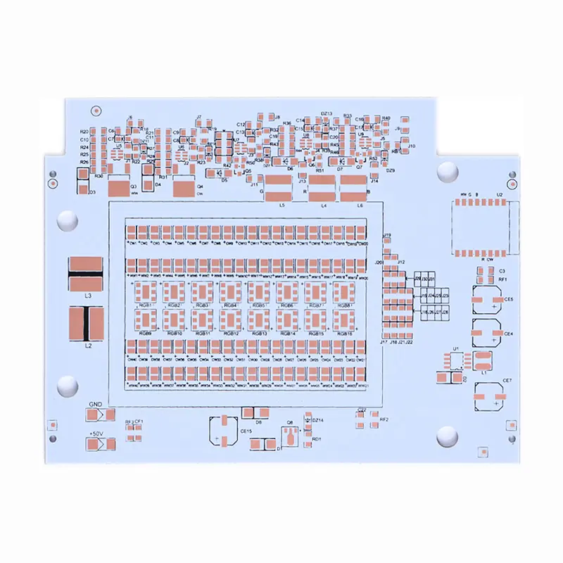 Aluminum
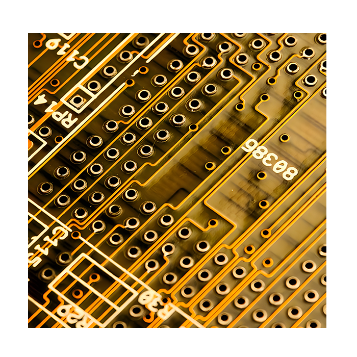 Copper Core
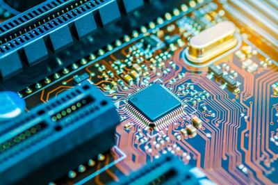 PCB Assembly
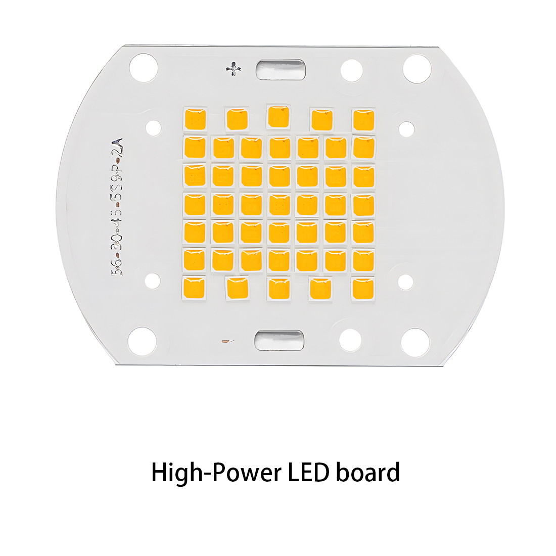 LED light PCBA
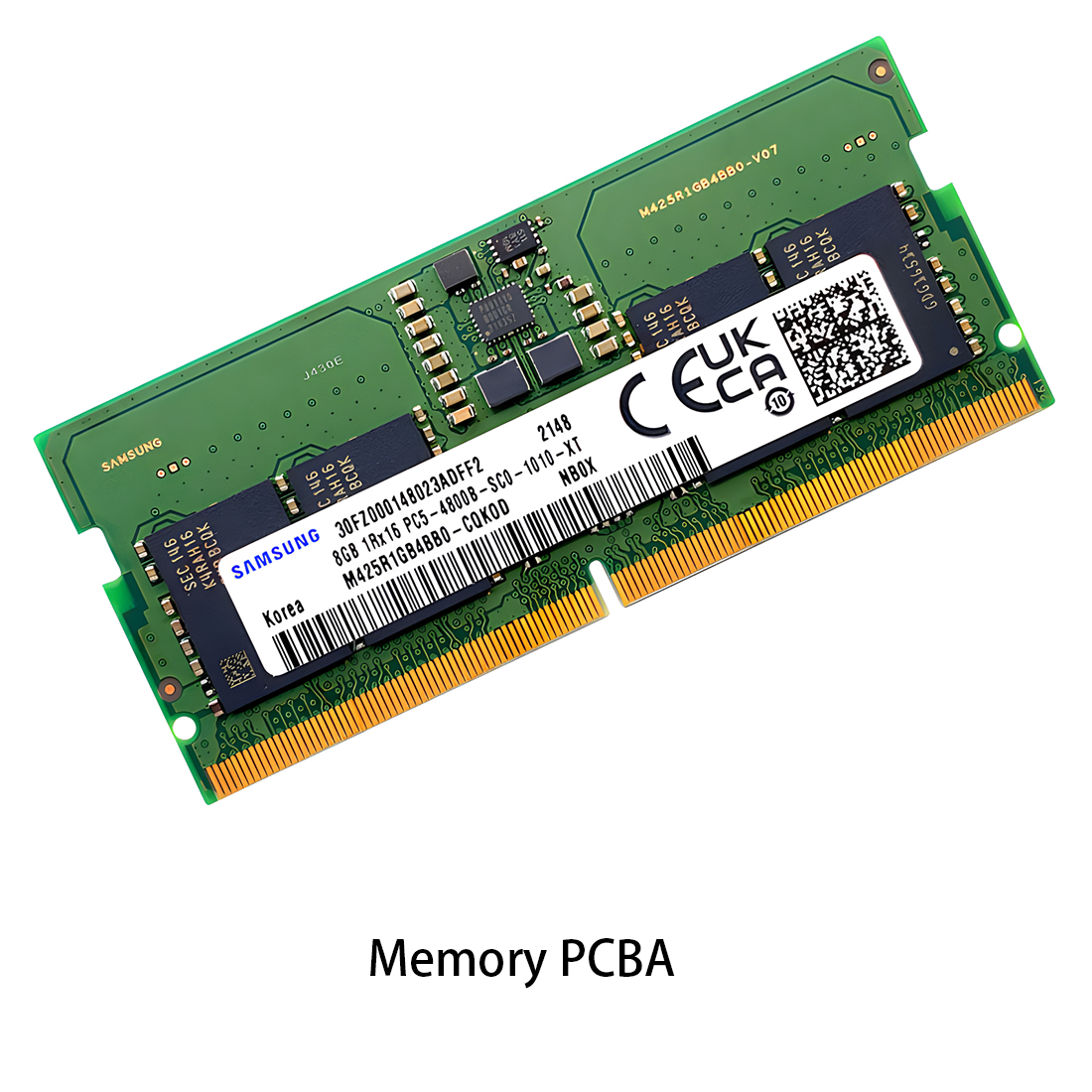 Memory PCBA
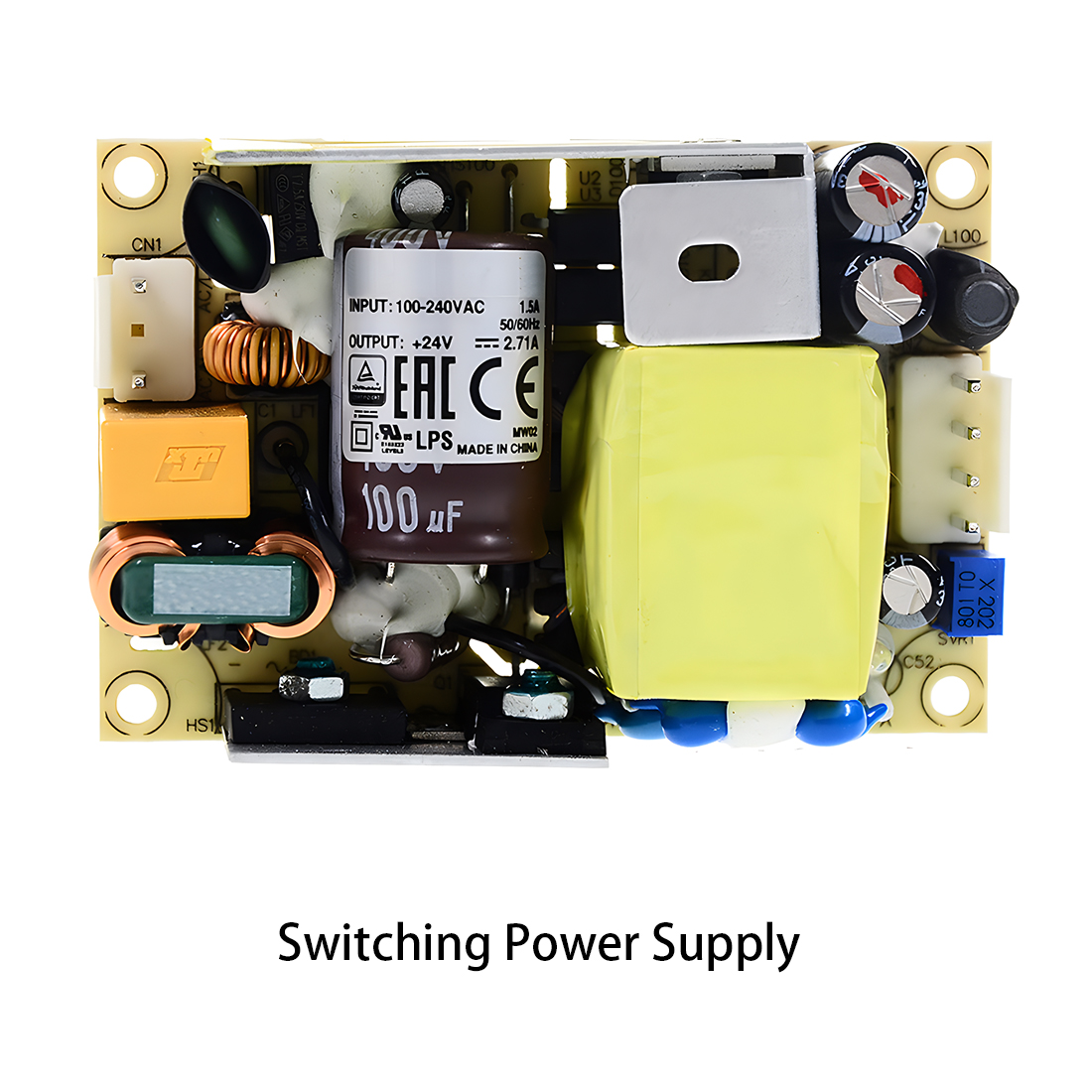 Power Supply PCBA
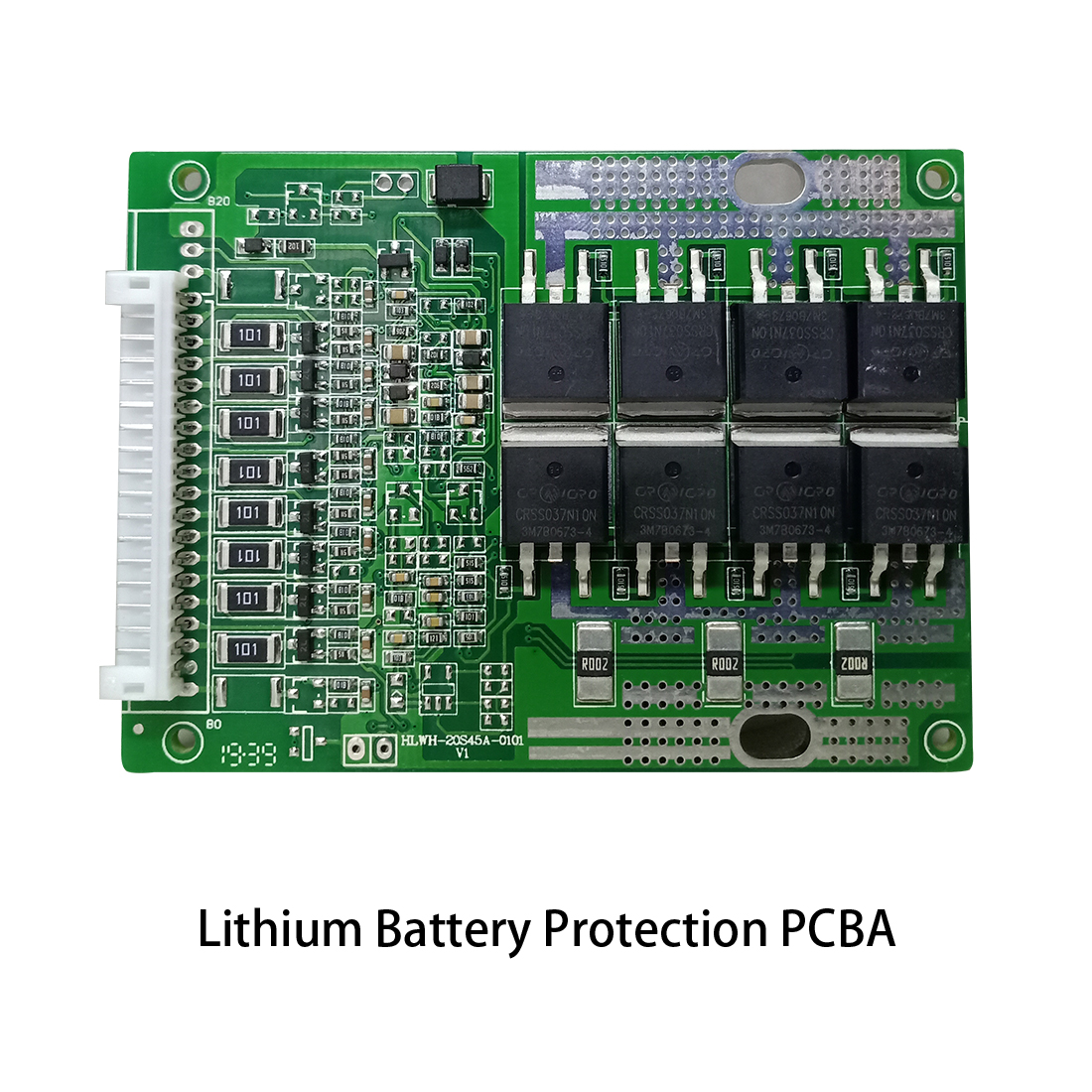 New Energey PCBA
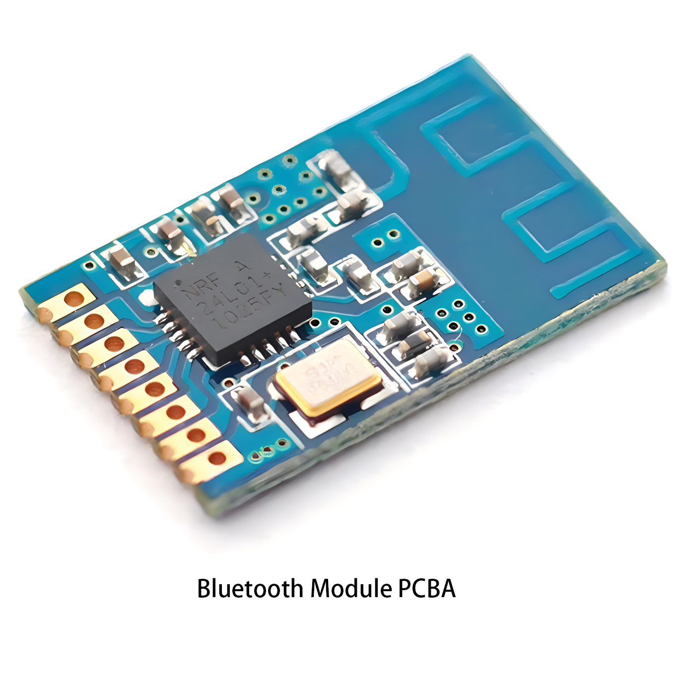 Communication PCBA
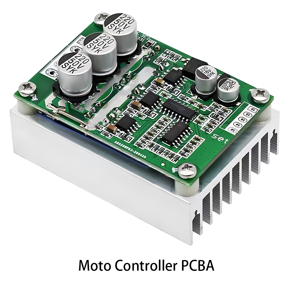 Industrial Control PCBA
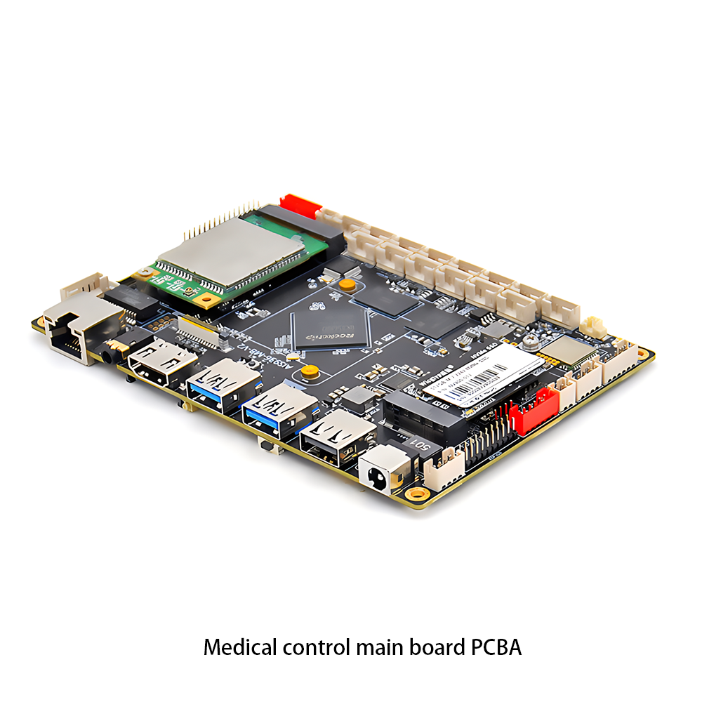 Medical Equipment PCBA
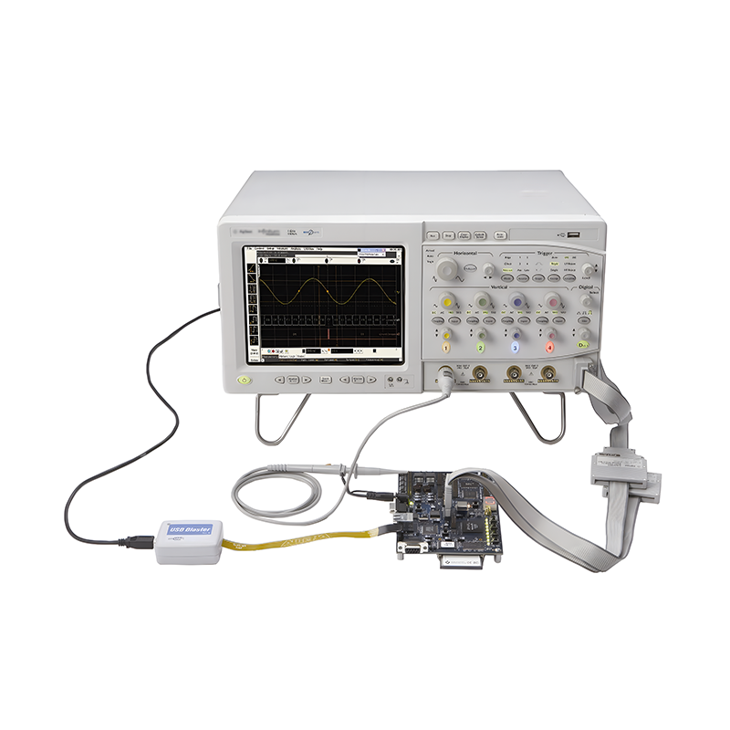 PCBA Testing Service
 Certification Application
 RoHS Certification Application
 REACH Certification Application
 CE Certification Application
 FCC Certification Application
 CQC Certification Application
 UL Certification Application
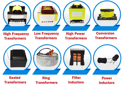 Transformers, Inductors
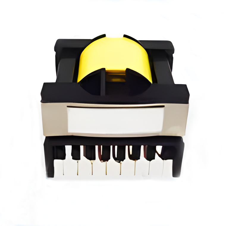 High Frequency Transformers
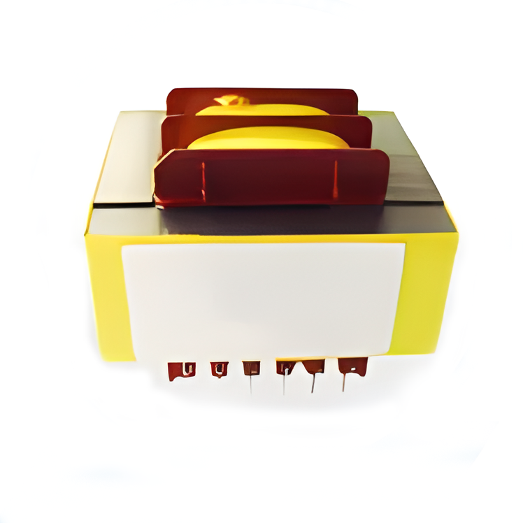 Low Frequency Transformers
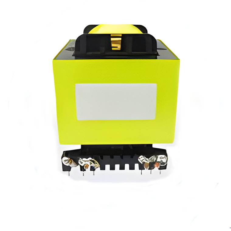 High Power Transformers
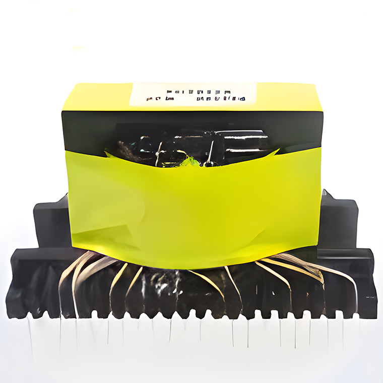 Conversion Transformers
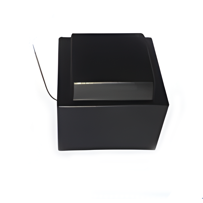 Sealed Transformers
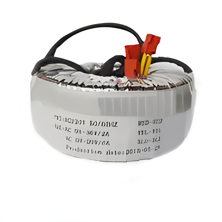 Ring Transformers
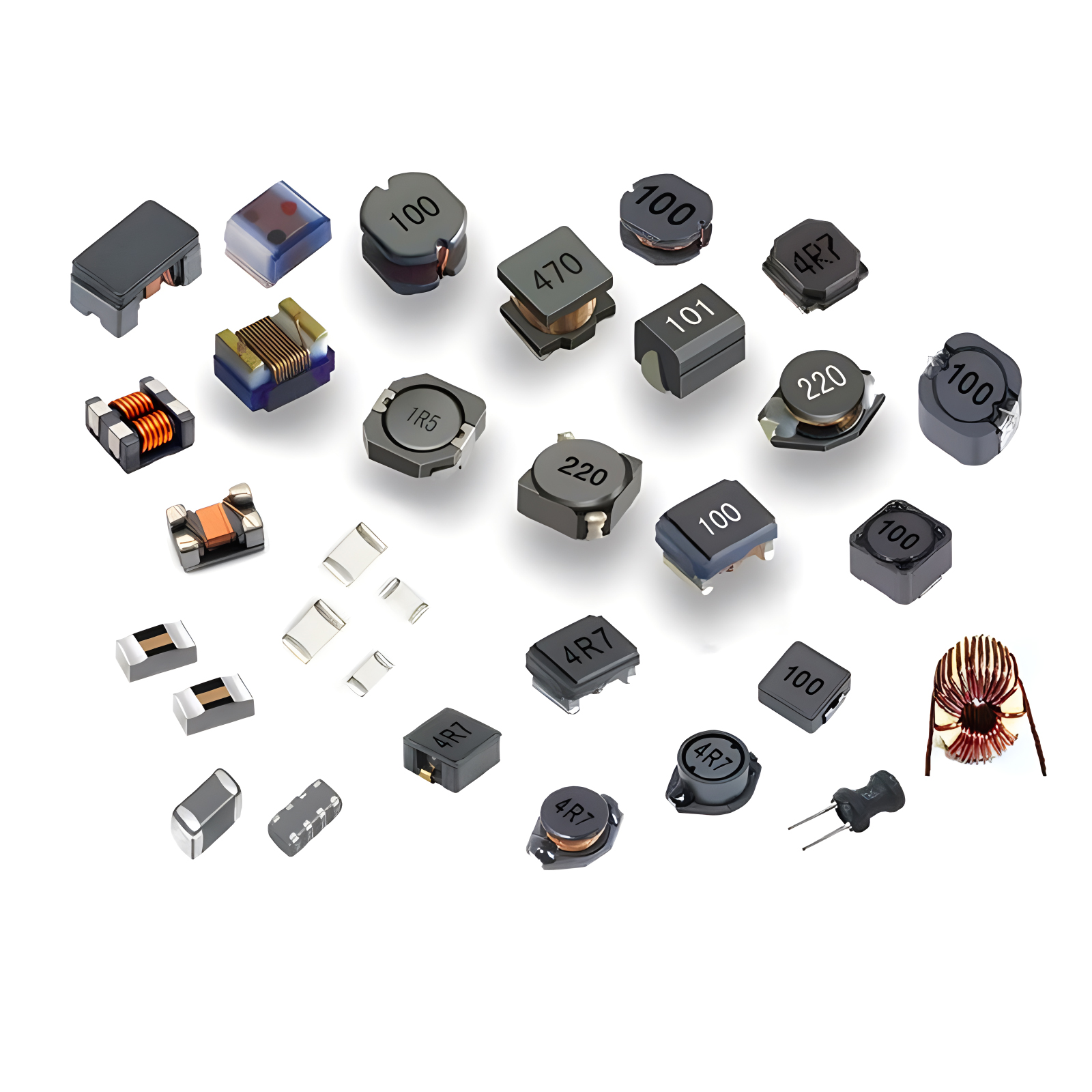 Inductors
 Wires,Cables Customized
 Network Cables
 Power Cords
 Antenna Cables
 Coaxial Cables
 Net Position Indicator(网位仪)
 Capacitors
 Connectors
 Diodes
 Embedded Processors & Controllers
 Digital Signal Processors (DSP/DSC)
 Microcontrollers (MCU/MPU/SOC)
 Programmable Logic Device(CPLD/FPGA)
 Communication Modules/IoT
 Resistors
 Through Hole Resistors
 Resistor Networks, Arrays
 Potentiometers,Variable Resistors
 Aluminum Case,Porcelain Tube Resistance
 Current Sense Resistors,Shunt Resistors
 Switches
 Transistors
 Power Modules
 Isolated Power Modules
 DC-AC Module(Inverter)
 RF and Wireless