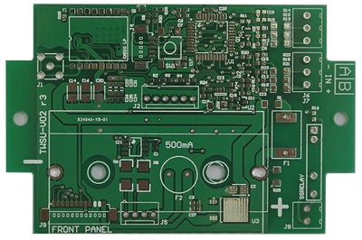
 PCB
PCB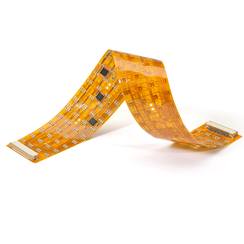 FPC
FPC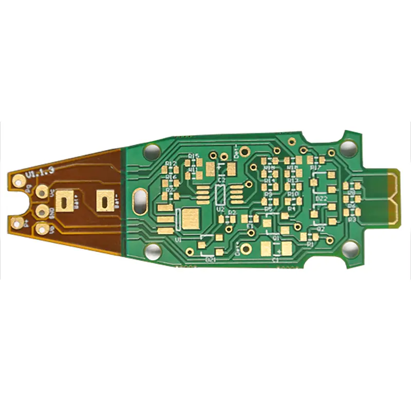 Rigid-Flex
 FR-4
FR-4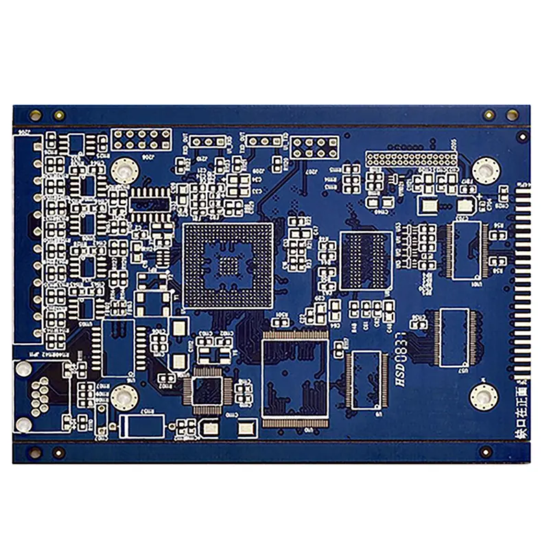 HDI PCB
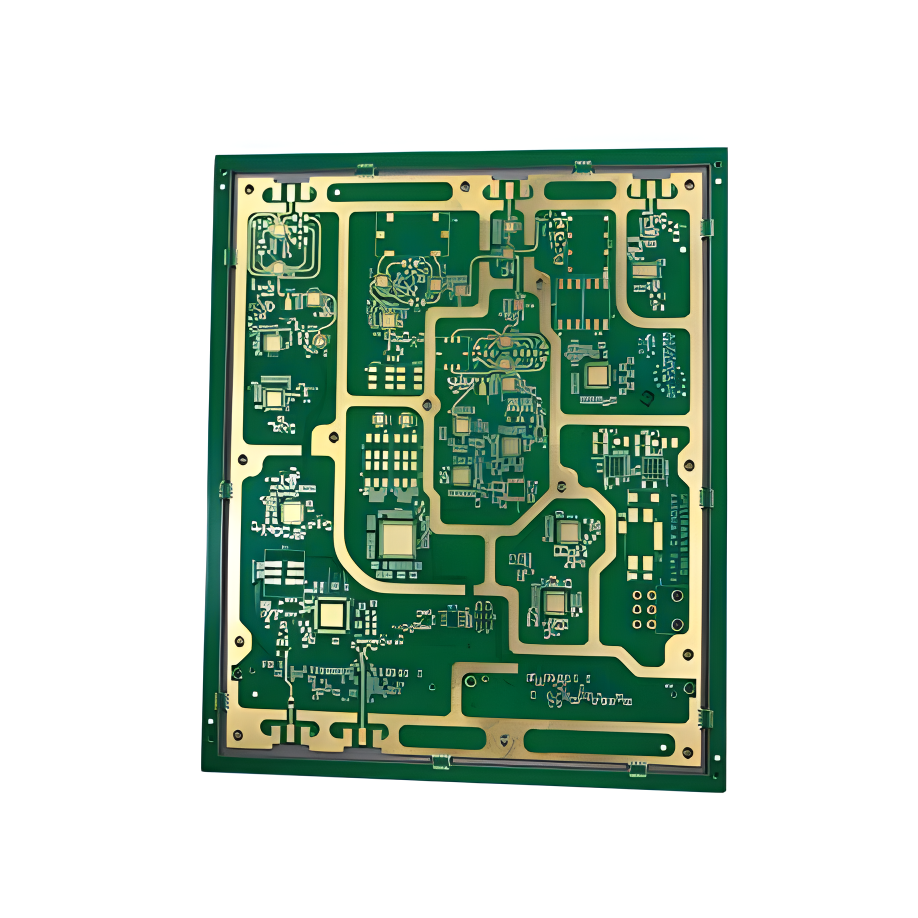 Rogers High-Frequency Board
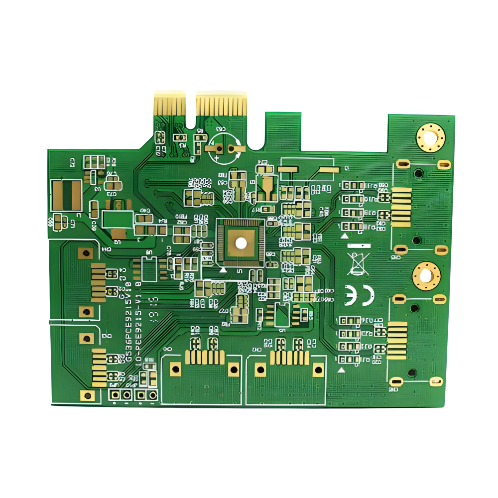 PTFE Teflon High-Frequency Board
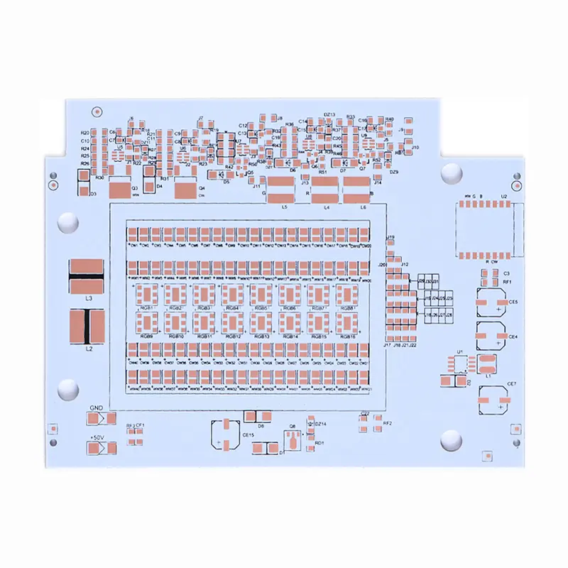 Aluminum
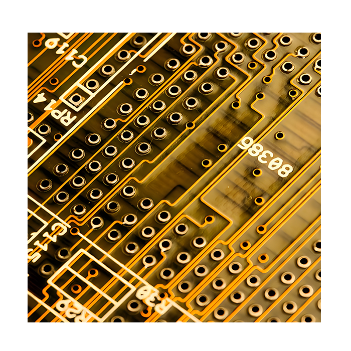 Copper Core
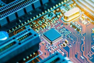 PCB Assembly
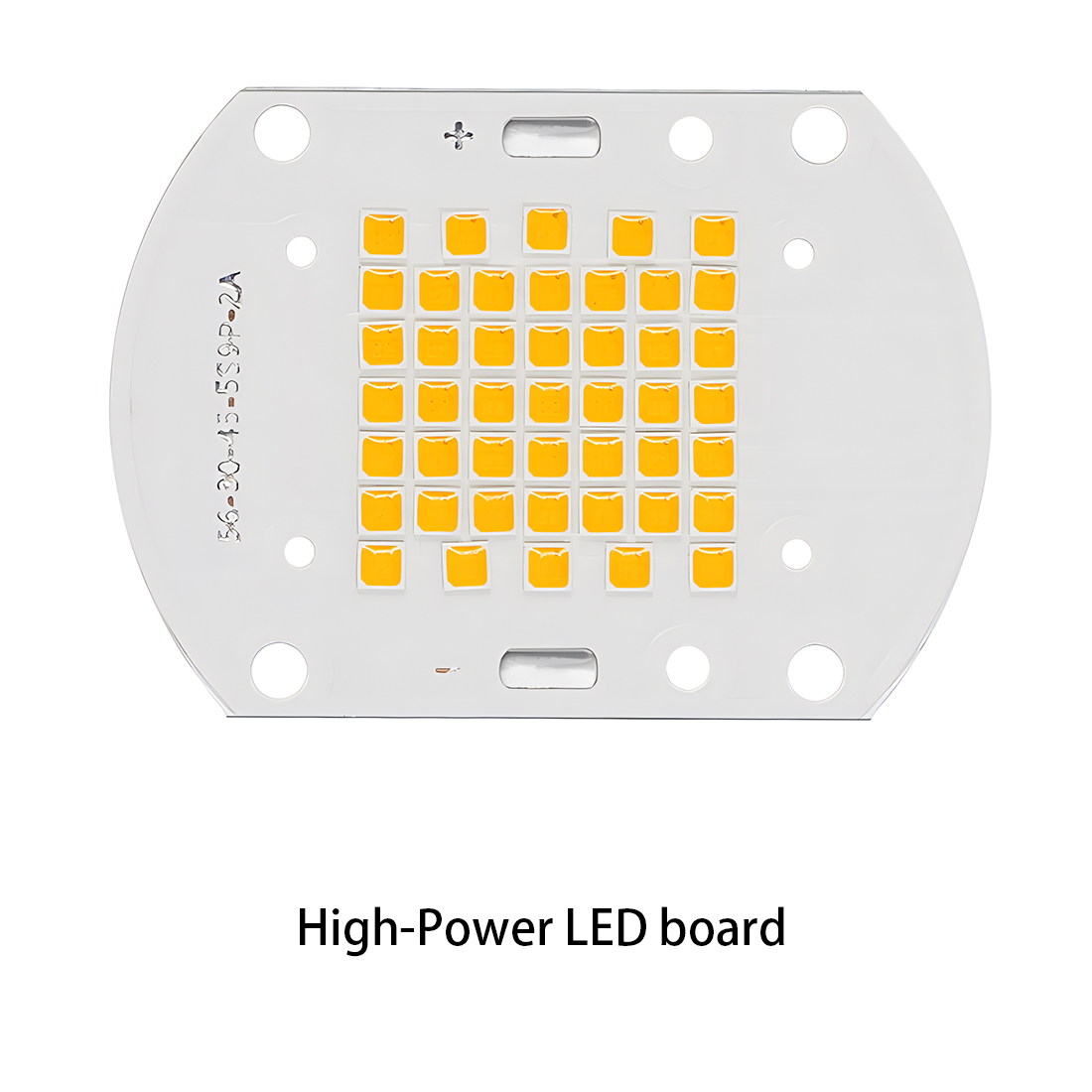 LED light PCBA
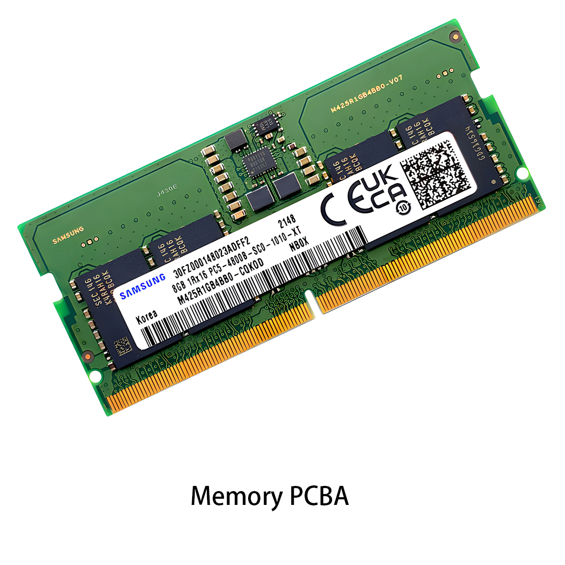 Memory PCBA
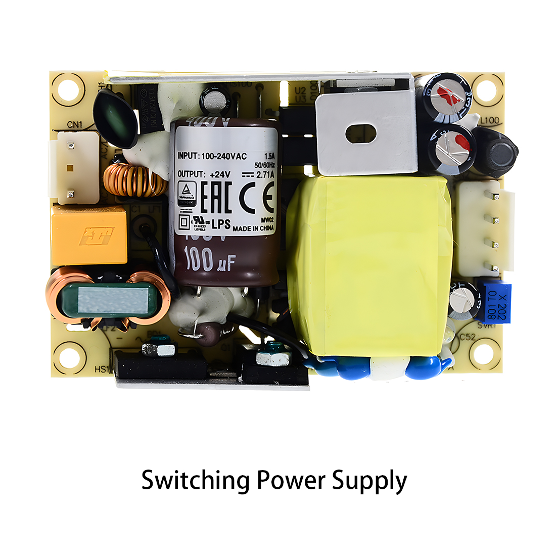 Power Supply PCBA
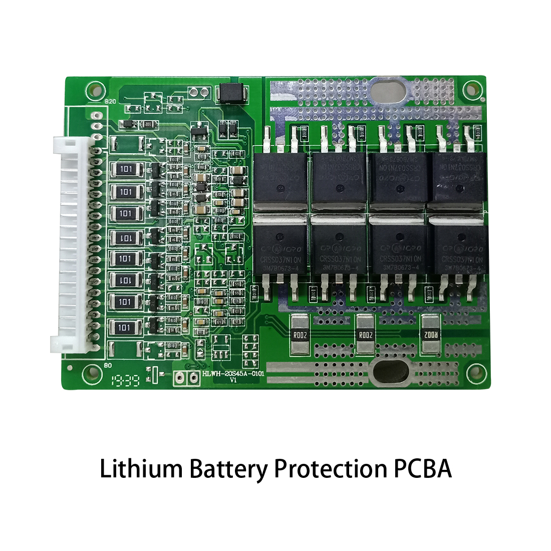 New Energey PCBA
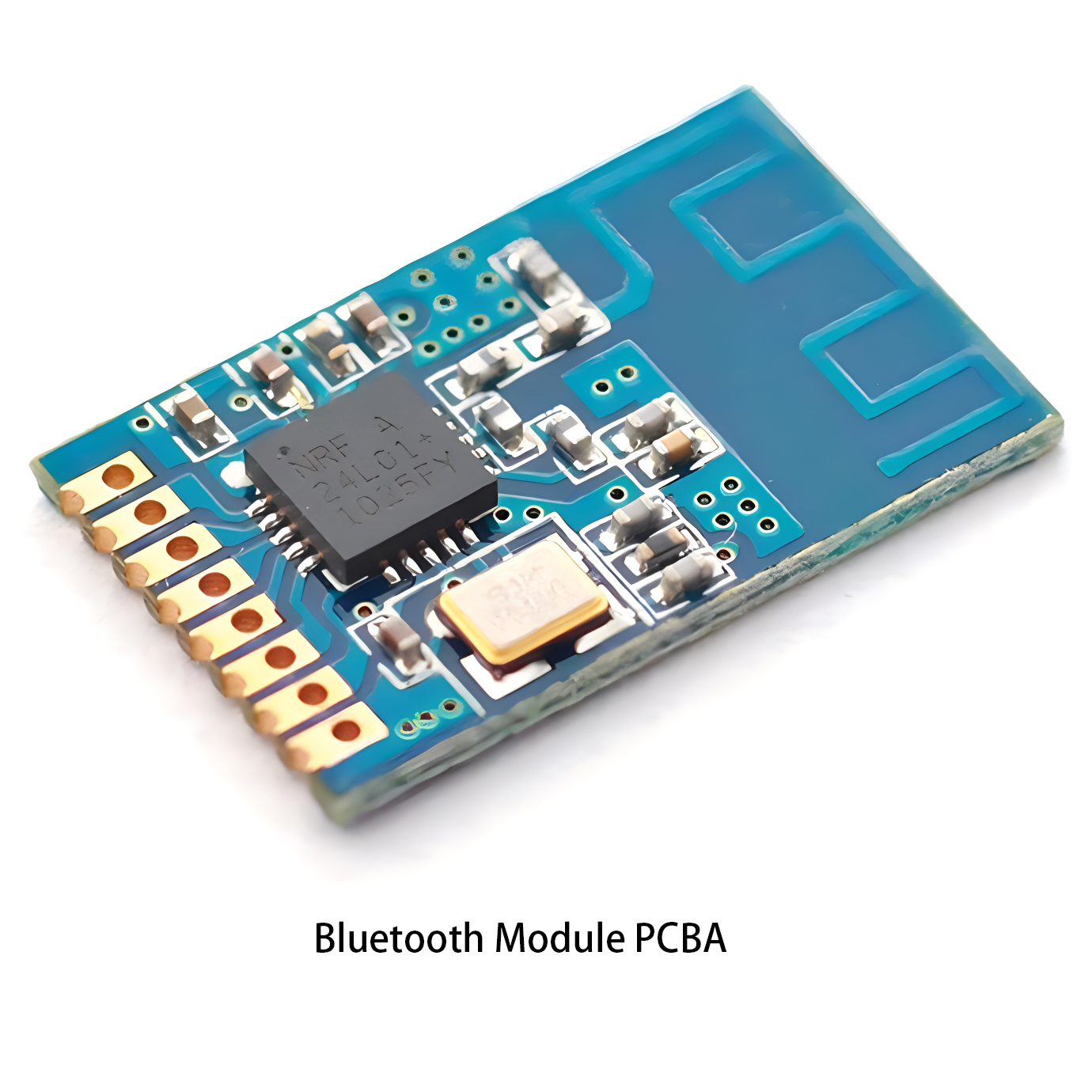 Communication PCBA
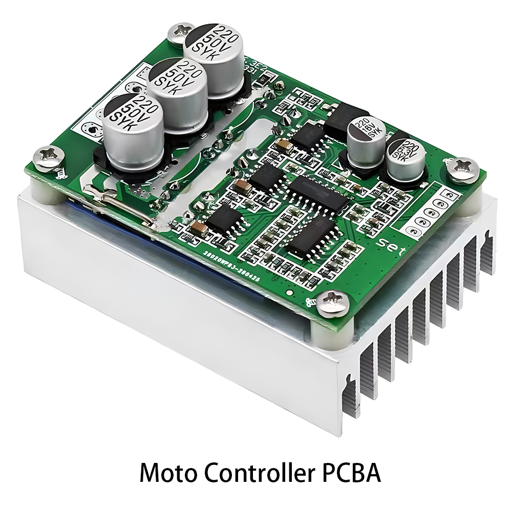 Industrial Control PCBA
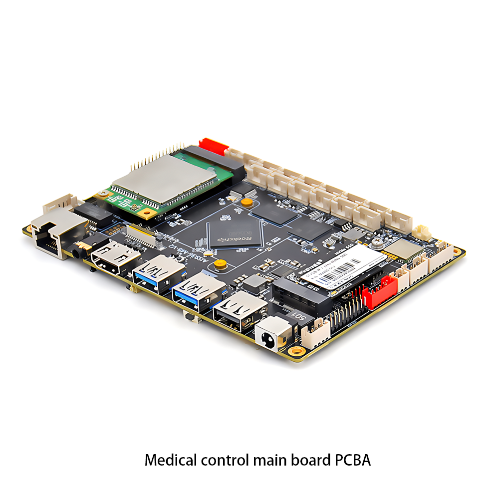 Medical Equipment PCBA
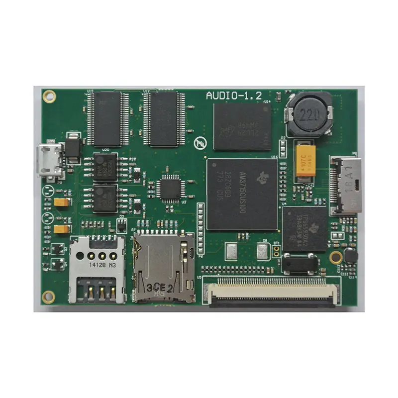 Testing Service
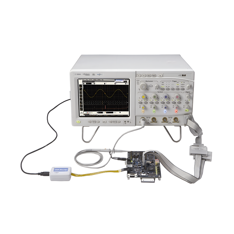 PCBA Testing Service
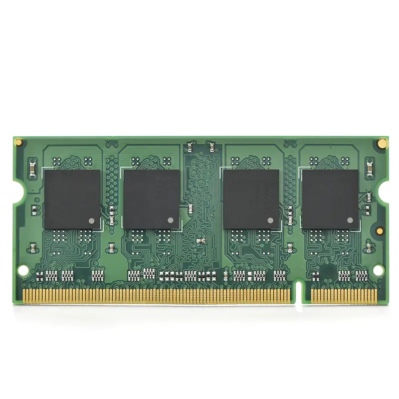 Certification Application
 RoHS Certification Application
 REACH Certification Application
 CE Certification Application
 FCC Certification Application
 CQC Certification Application
 UL Certification Application
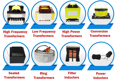 Transformers
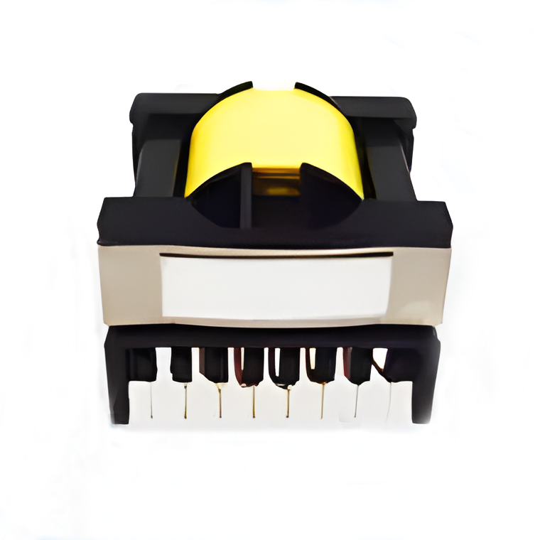 High Frequency Transformers
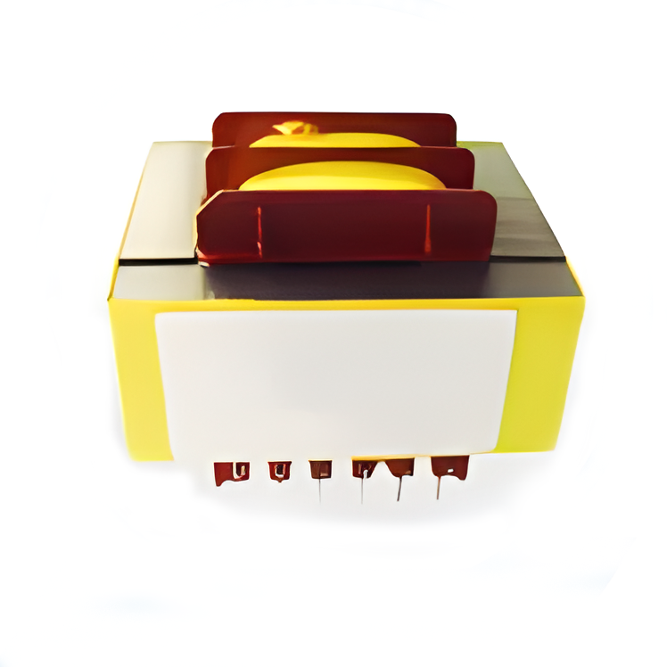 Low Frequency Transformers
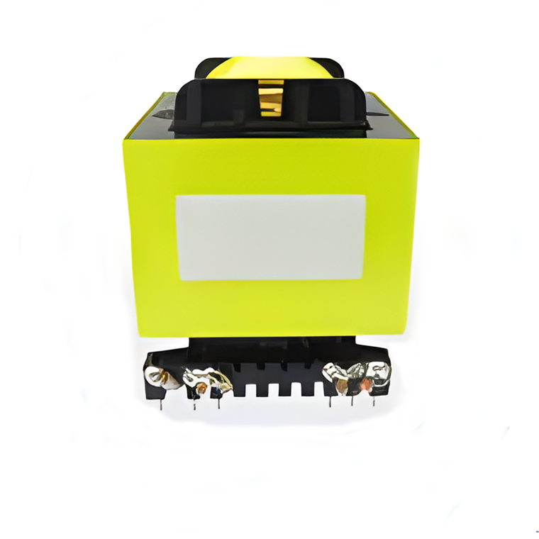 High Power Transformers
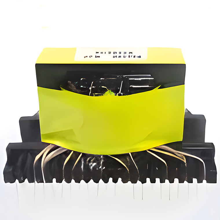 Conversion Transformers
 Sealed Transformers
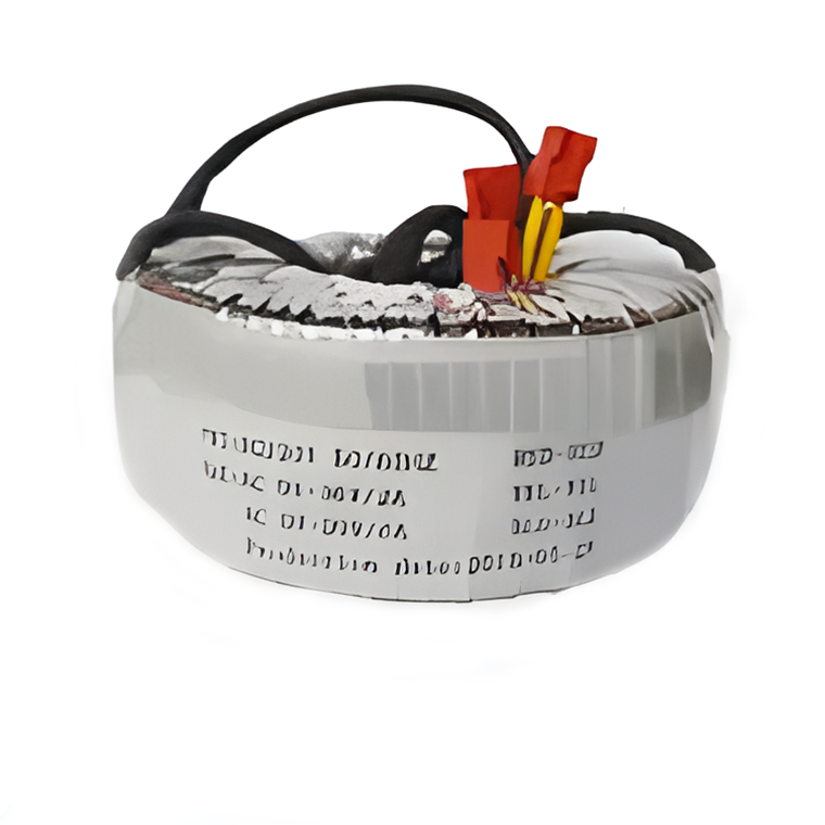 Ring Transformers
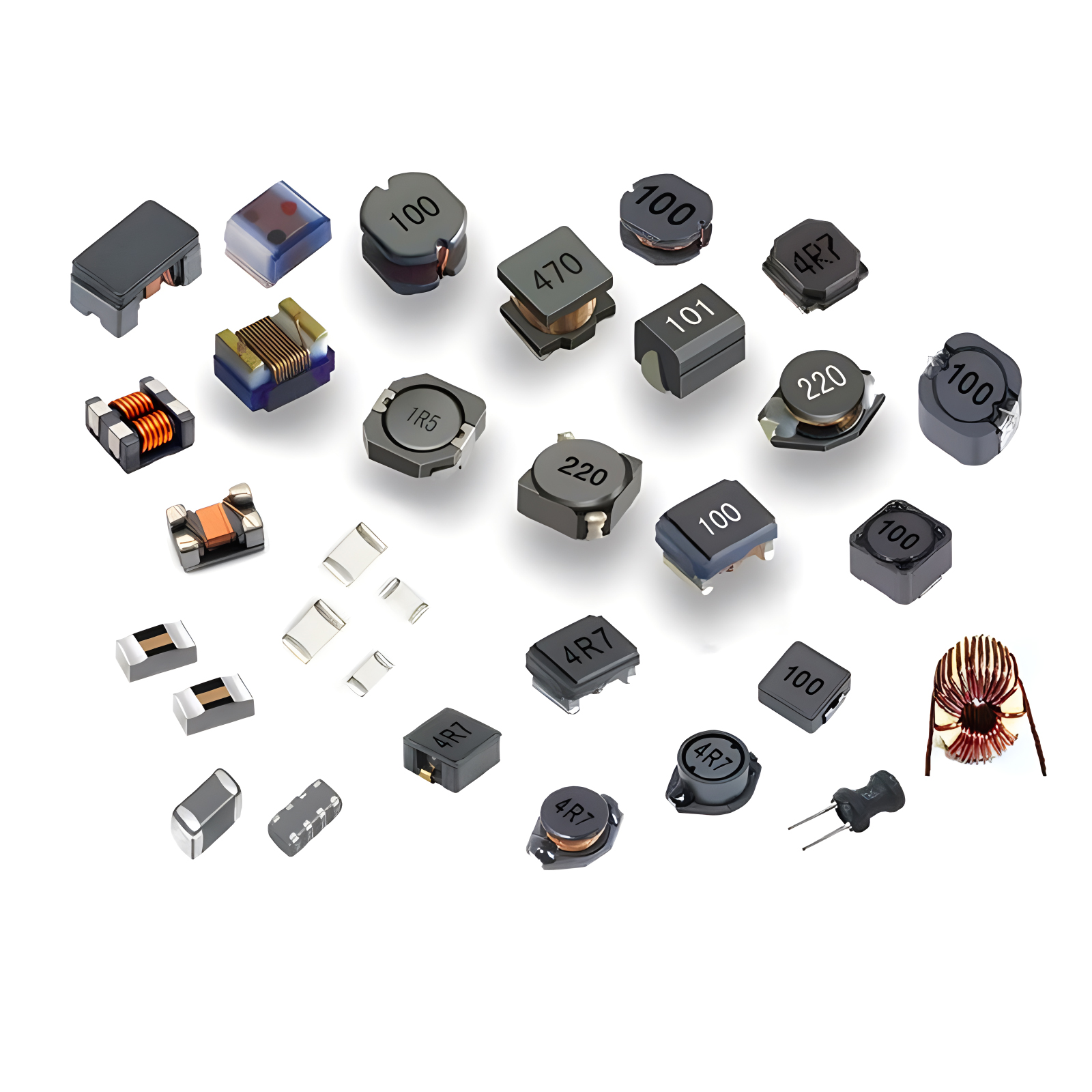 Inductors
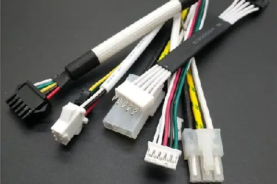 Wires,Cables Customized
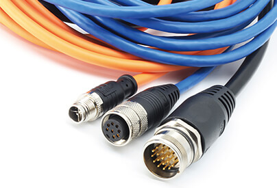 wires-cables
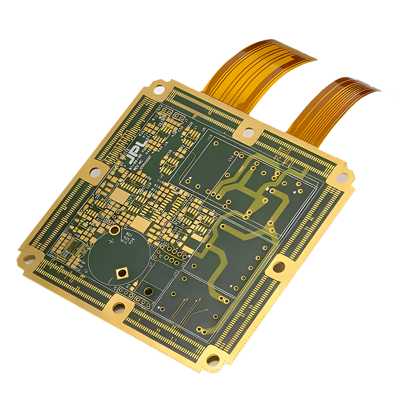
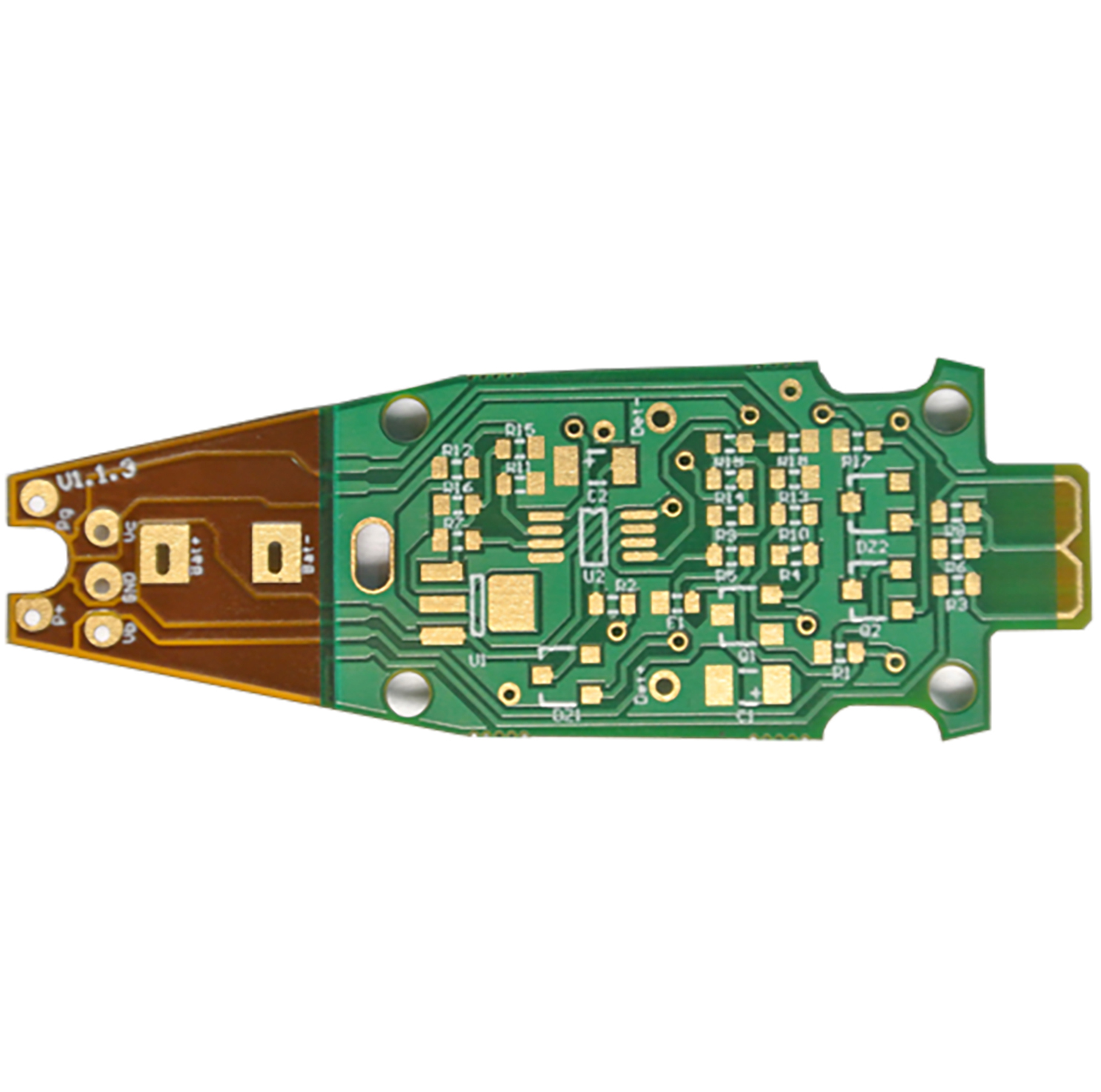


Rigid-Flex PCB consumer electronics PCB

Rigid-Flex PCB
Performance-wise, Rigid-Flex PCBs excel in applications demanding a combination of flexibility and structural integrity. The flexible portions allow the board to bend and fold, enabling intricate three-dimensional designs and conforming to the shape of the device. This flexibility reduces the need for additional connectors and wiring, enhancing reliability and reducing overall weight. The rigid sections provide stability and support for components that require a solid foundation.
The applications of Rigid-Flex PCBs are diverse and extend across industries such as aerospace, medical devices, and consumer electronics. Their unique design makes them ideal for devices where space optimization, weight reduction, and durability are critical factors. Common applications include wearable devices, aerospace instrumentation, and medical implants, where the combination of rigid and flexible elements accommodates the dynamic requirements of the application.
Interested?
Let us know more about your project.
REQUEST A QUOTE