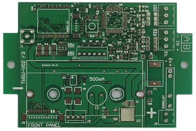
 PCB
PCB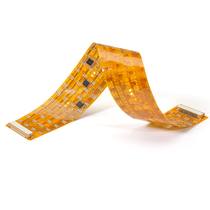 FPC
FPC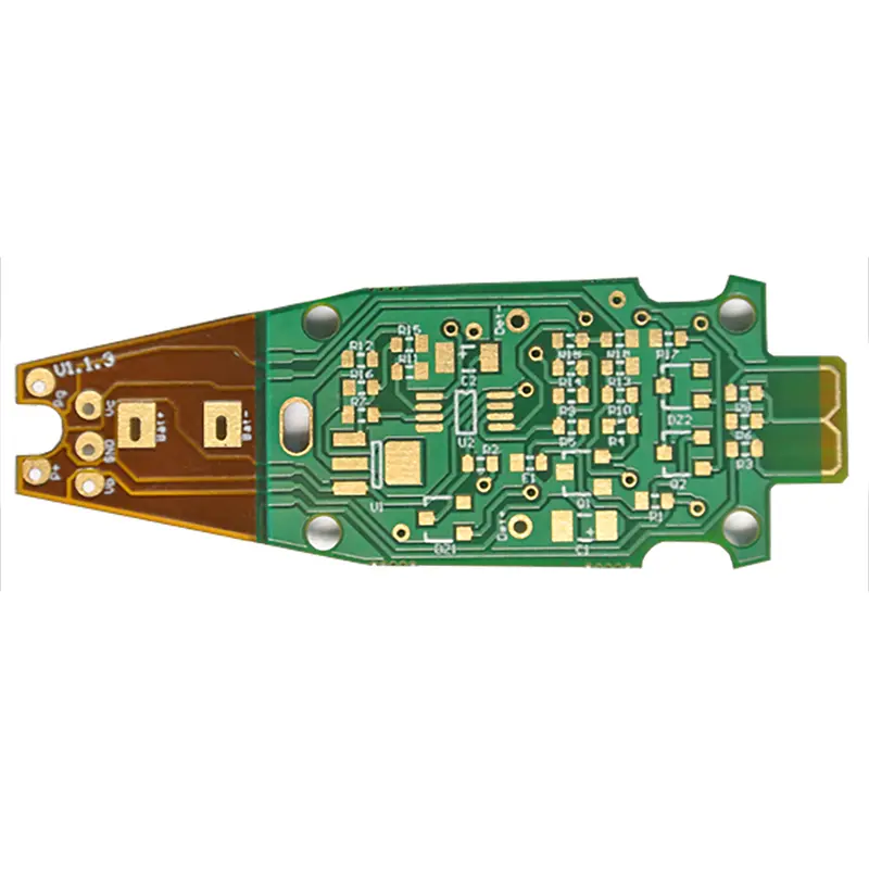 Rigid-Flex
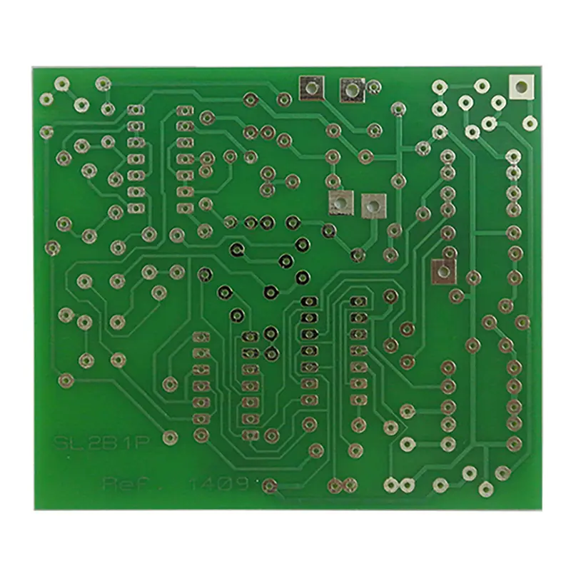 FR-4
FR-4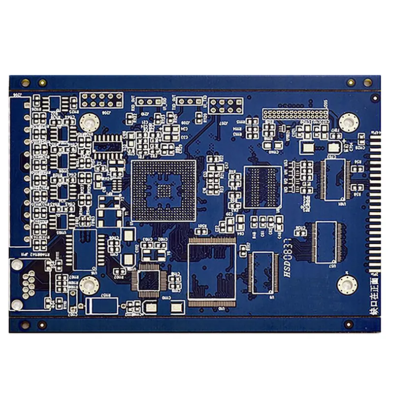 HDI PCB
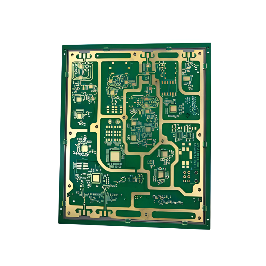 Rogers High-Frequency Board
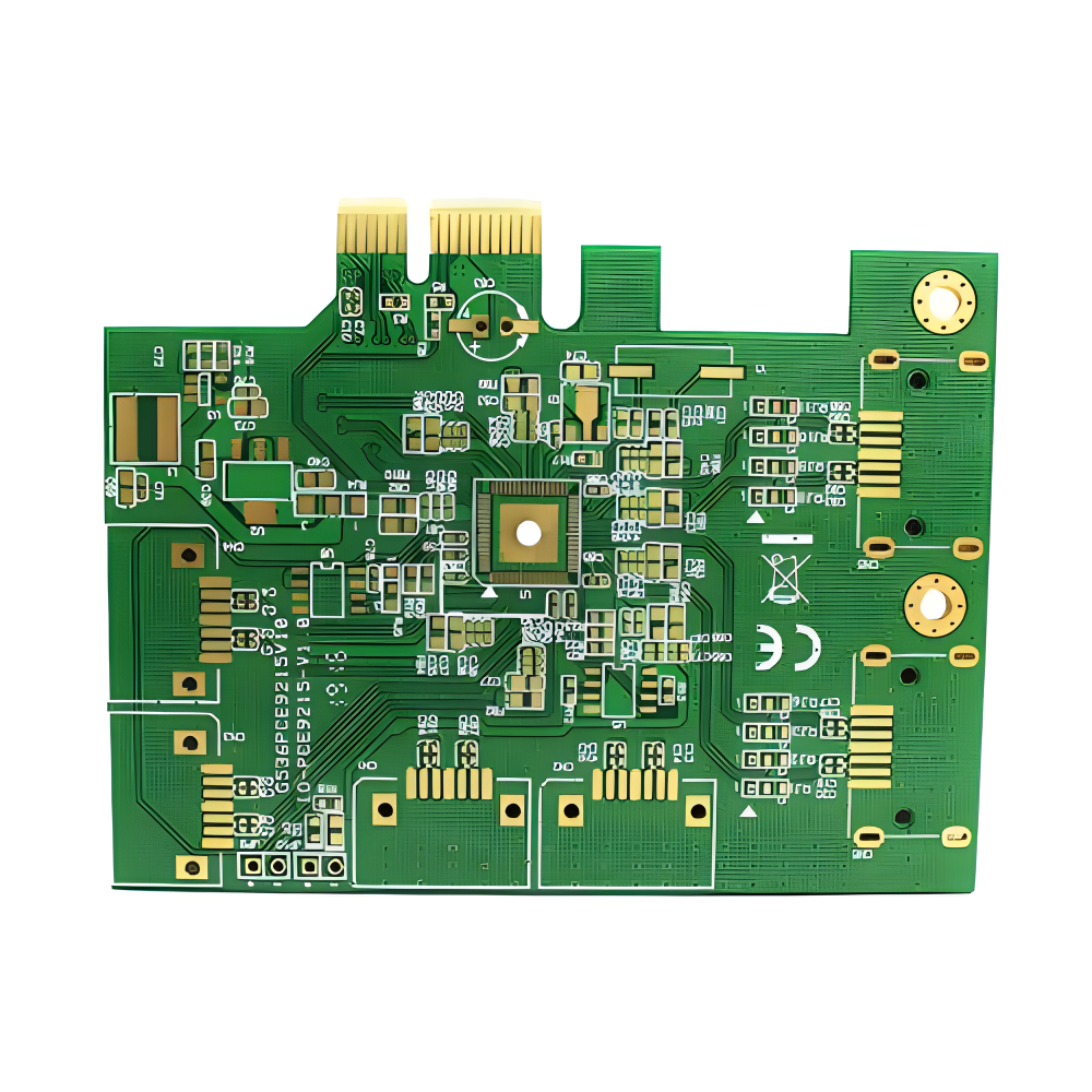 PTFE Teflon High-Frequency Board
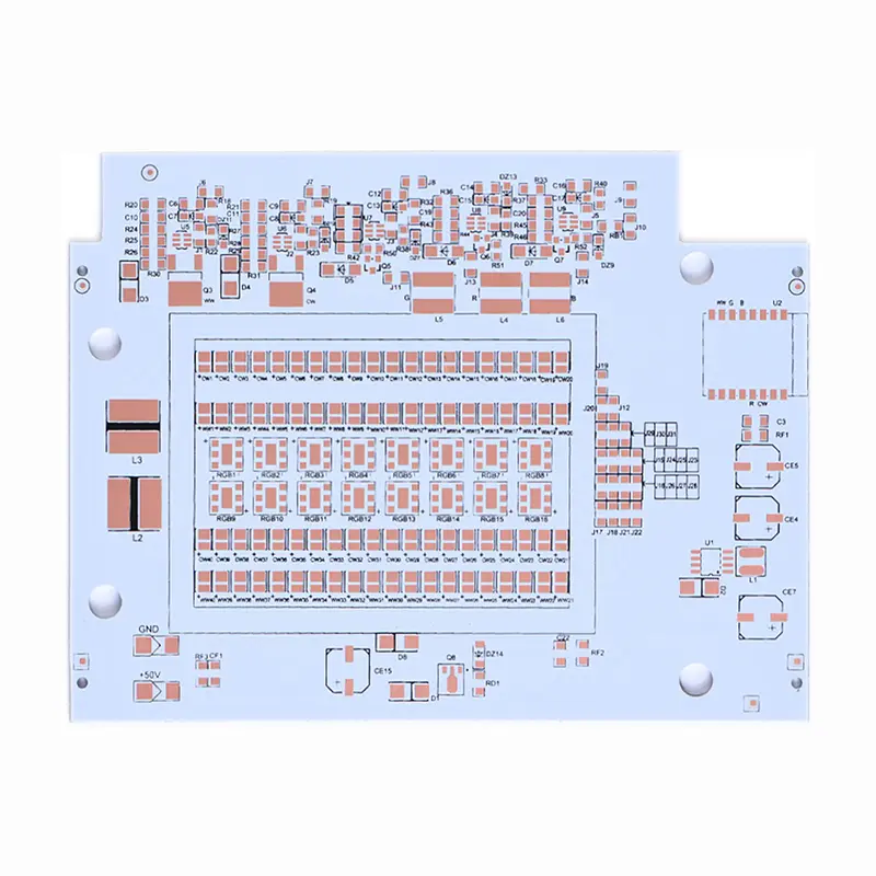 Aluminum
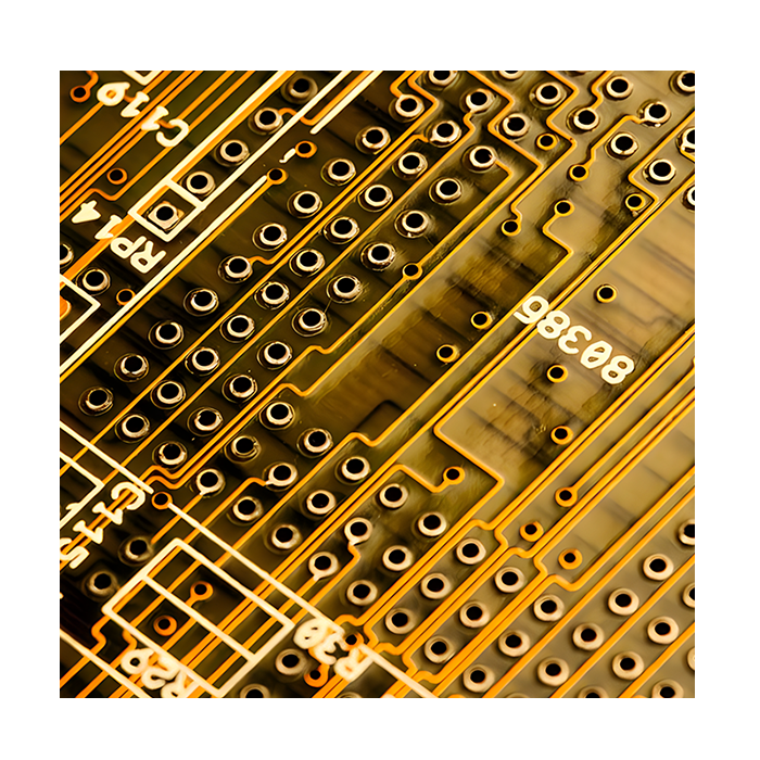 Copper Core
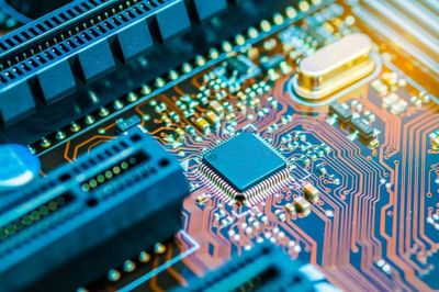 PCB Assembly
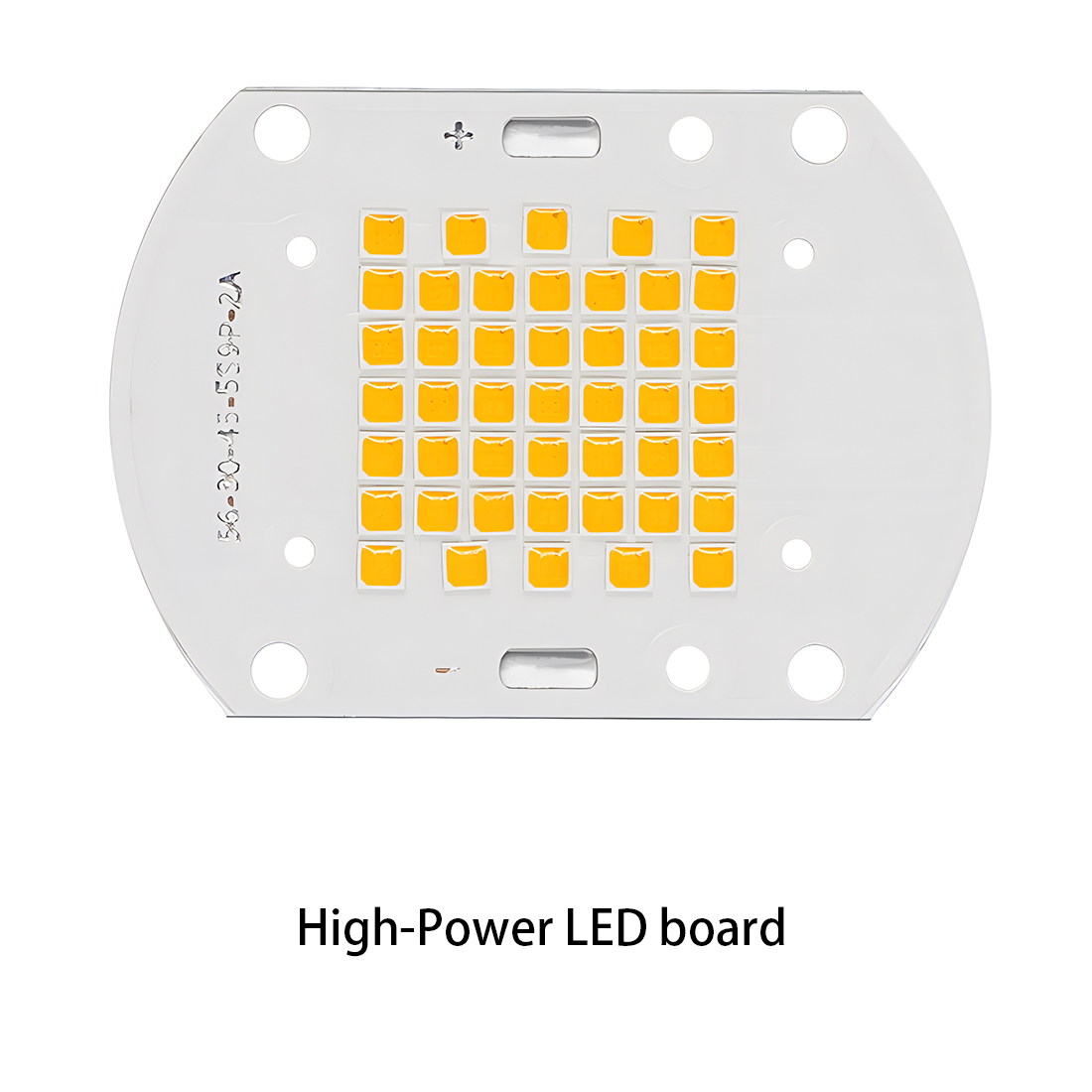 LED light PCBA
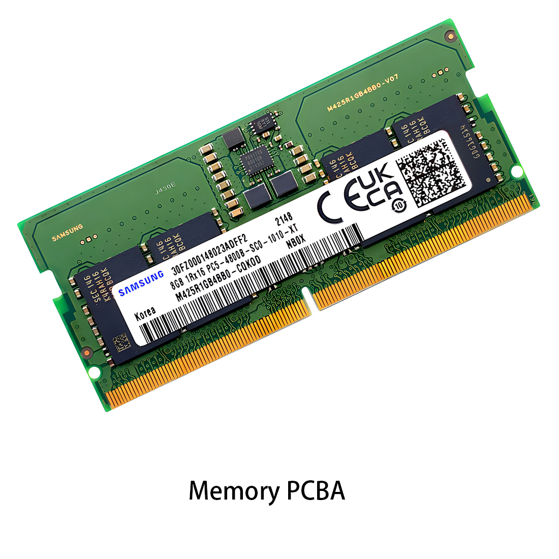 Memory PCBA
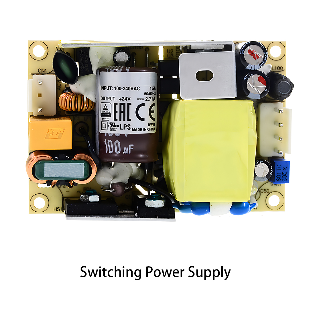 Power Supply PCBA
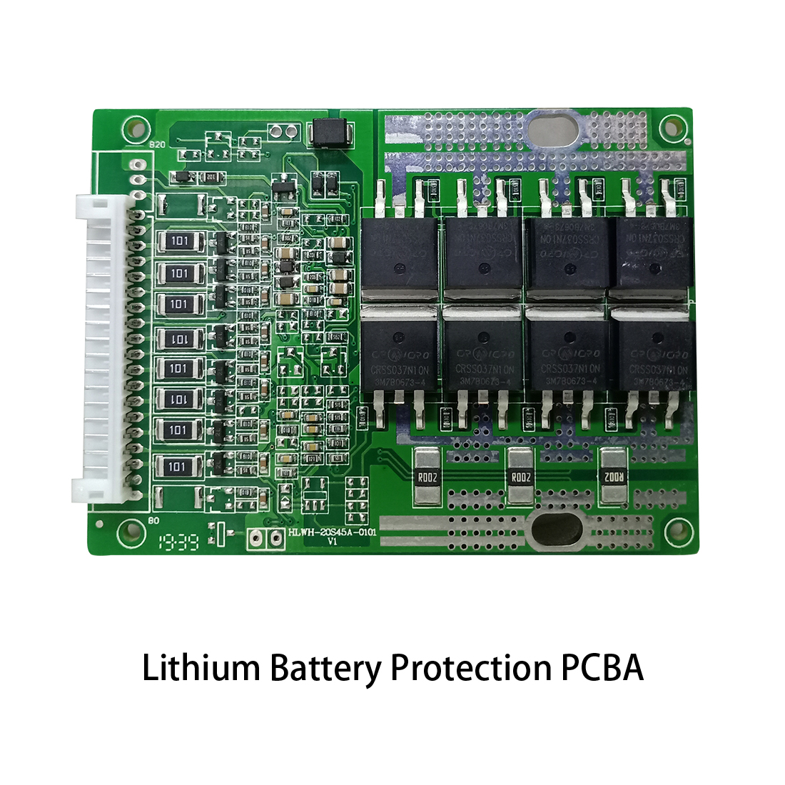 New Energey PCBA
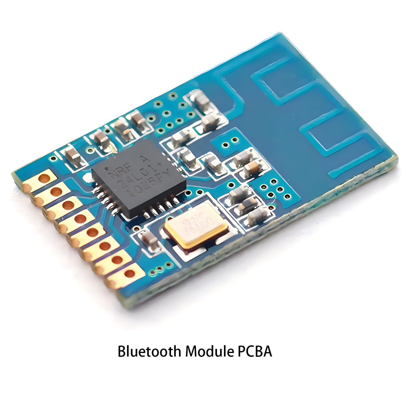 Communication PCBA
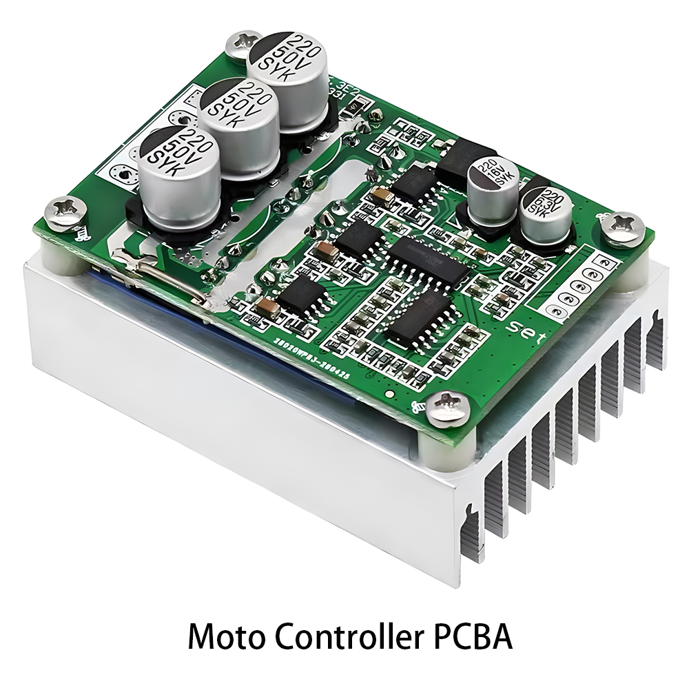 Industrial Control PCBA
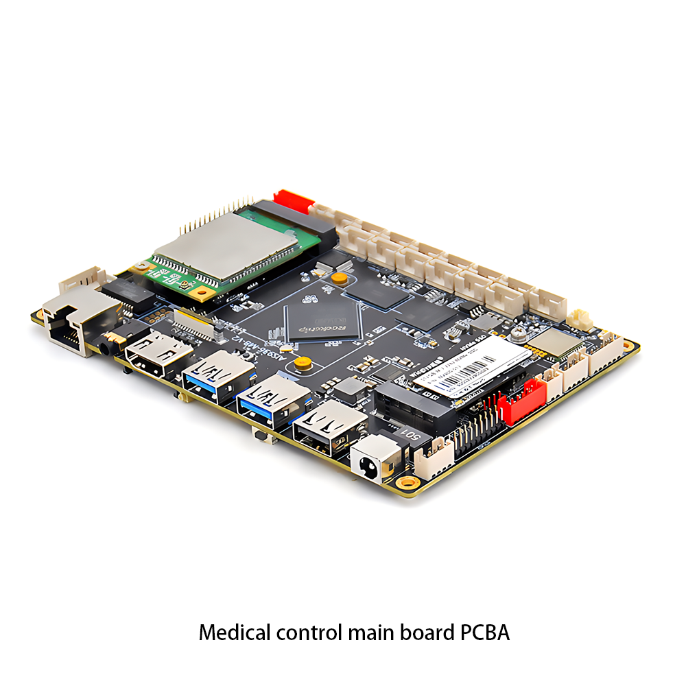 Medical Equipment PCBA
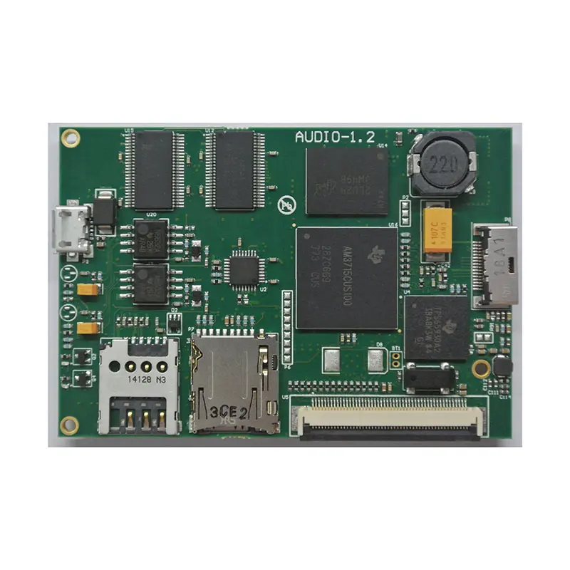 Testing Service
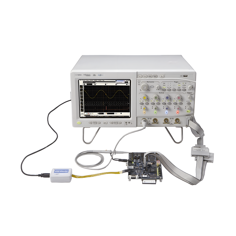 PCBA Testing Service
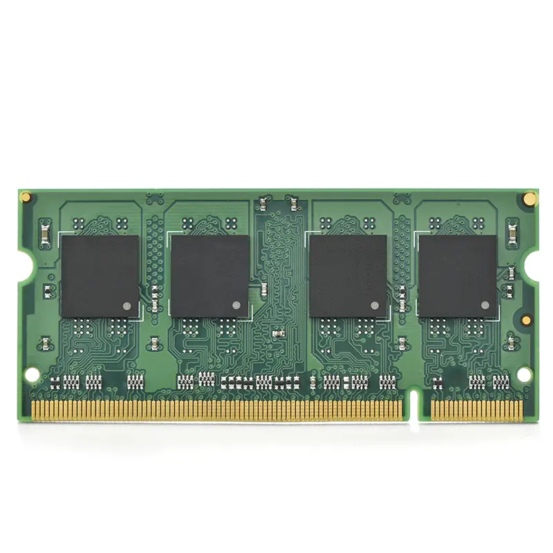 Certification Application
 RoHS Certification Application
 REACH Certification Application
 CE Certification Application
 FCC Certification Application
 CQC Certification Application
 UL Certification Application
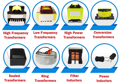 Transformers
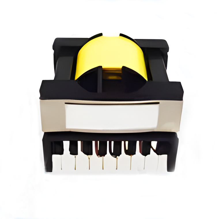 High Frequency Transformers
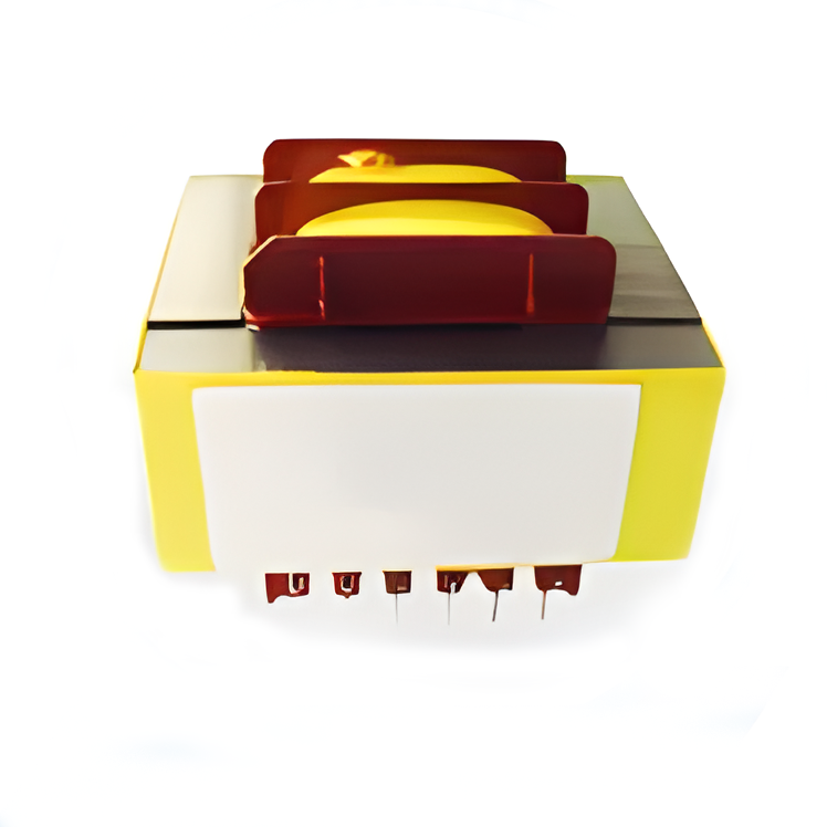 Low Frequency Transformers
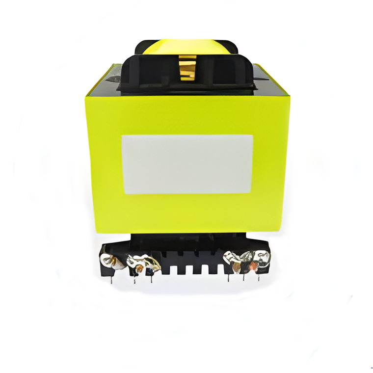 High Power Transformers
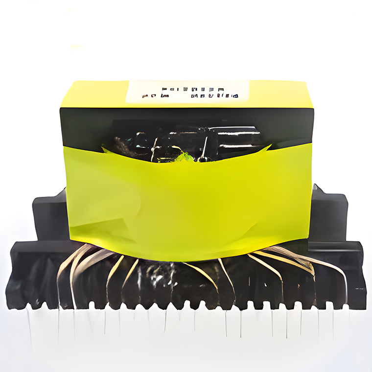 Conversion Transformers
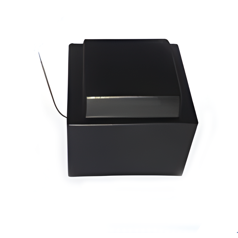 Sealed Transformers
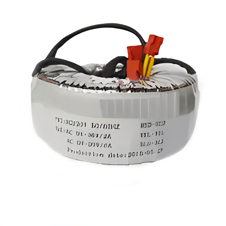 Ring Transformers
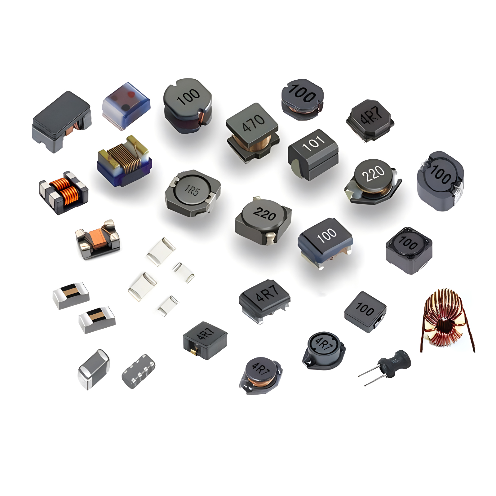 Inductors
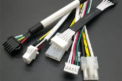 Wires,Cables Customized
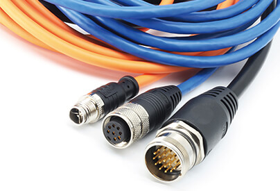 wires-cables
Company Profile
Minintel Technology Co., LimitedMinintel Technology Co., Limited was established in Zhongwu Industrial Park, Bao'an District, Shenzhen, China in 2007. After nearly two decades of development and accumulation, the company's PCB business has achieved the production capacity of "high multi-layer, high precision, high reliability, and various types", with the maximum number of layers reaching 42. It covers various board types such as FR-4 rigid boards, FPCs, rigid-flex boards, HDI PCBs, high-precision multilayer PCBs, high-frequency boards, thermoelectric separation copper substrates, aluminum substrates, and so on.
The company provides multi-dimensional production modes such as PCB, PCBA sampling, small-batch, and large-batch production, as well as technologies and services such as steel mesh/fixtures. It has established a complete PCB intelligent manufacturing system, creating solutions for the electronics and machinery industries with excellent technological capabilities, building an intelligent industrial ecosystem, and widely applying its products to computers, aerospace, automotive electronics, new energy (wind power, photovoltaic), big data centers, industrial interconnection, medical instruments, industrial control, and other fields, helping various industries achieve technological innovation.
Workshop
The fully automated production line is the solid foundation for our efficient production and timely delivery.

Solder paste printing
Fully automatic solder paste printing machines are equipped with an optical alignment system, which automatically aligns the stencil apertures with the PCB pads by recognizing the Mark points on the PCB, thus enabling fully automated operation.
Solder paste inspection
80% of the defects in SMT production come from poor solder paste printing, and fully automatic three-dimensional solder paste inspection (SPI) equipment can control printing defects to the greatest extent.
Component placement
With a maximum mounting speed of 45,000 components per hour, it is still capable of efficiently and accurately placing high-precision components such as BGA.
Plug-in welding
Selective wave soldering can set the welding parameters for each solder joint, allowing for better process adjustments based on the points to be soldered, greatly improving the reliability of soldering.
Image detection
AOI (Automated Optical Inspection) is an automated optical inspection system that uses optical principles to detect defects encountered during welding production.
Radiographic testing
Automatic X-ray detection technology can detect invisible solder joints BGA, IC chips, CPUs, etc., and can also perform qualitative and quantitative analysis on the detection results to facilitate early detection of faults.
Three-proofing paint
The application of three-proofing paint can protect circuits/components from environmental factors such as moisture, contaminants, corrosion, and thermal cycling, while also improving the mechanical strength and insulation properties of the product.
Visual inspection
Using a high-magnification imaging system, we can observe the welding of components in all directions and strictly control product quality.