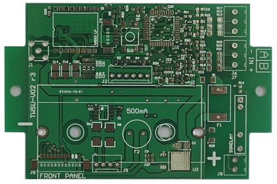
 PCB
PCB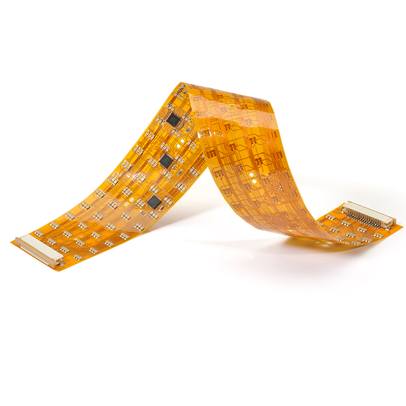 FPC
FPC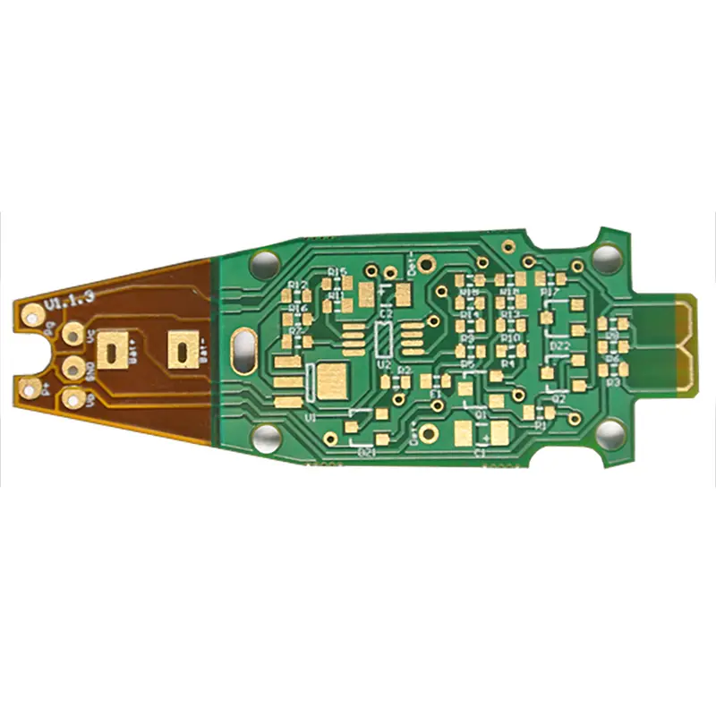 Rigid-Flex
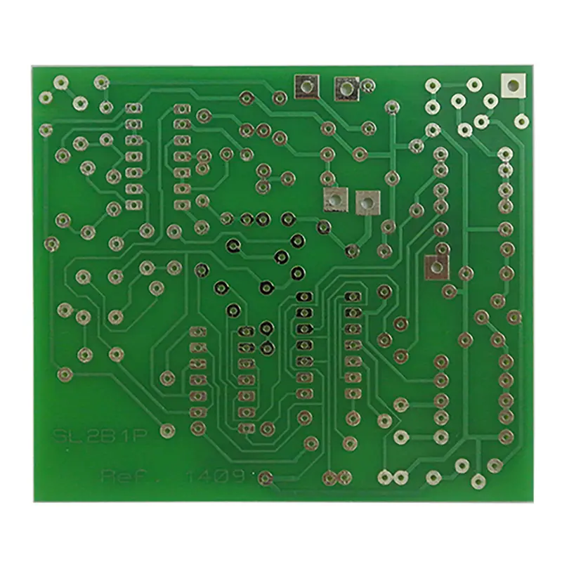 FR-4
FR-4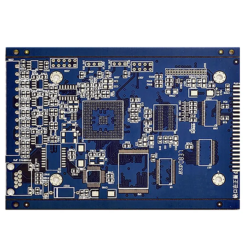 HDI PCB
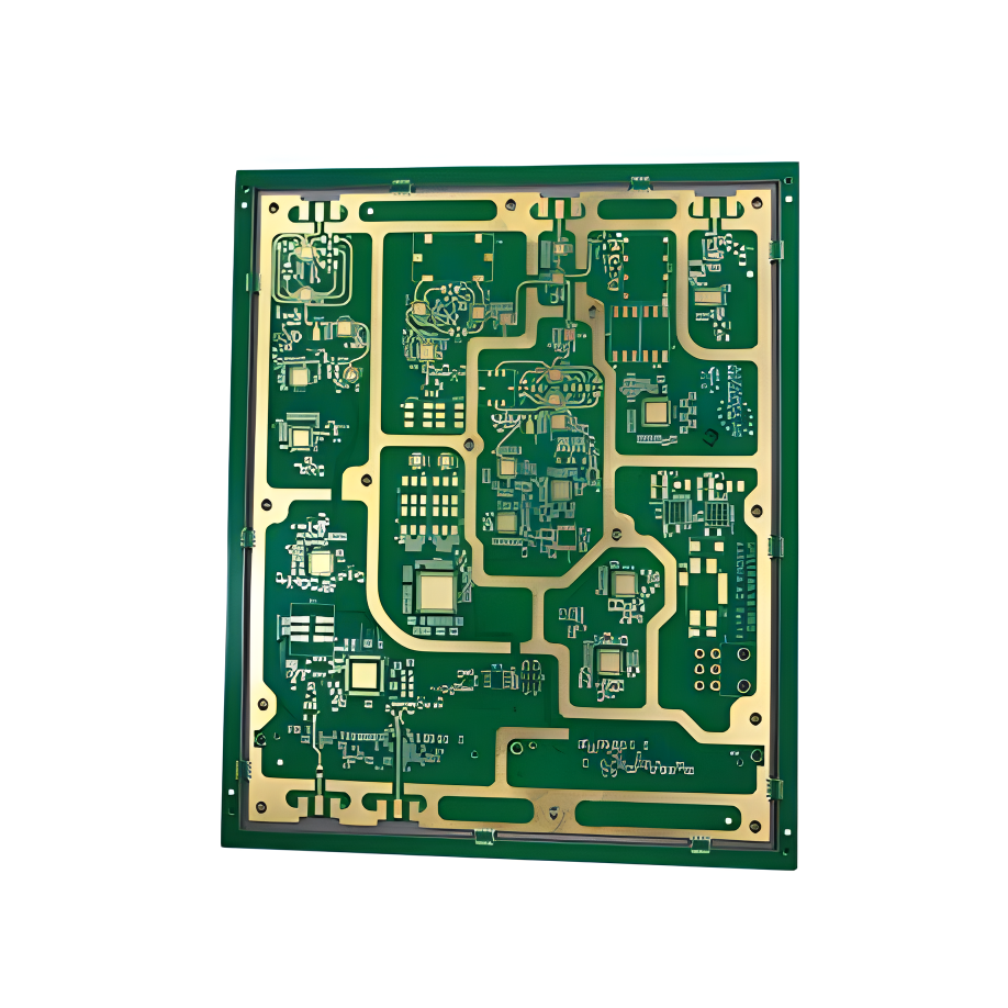 Rogers High-Frequency Board
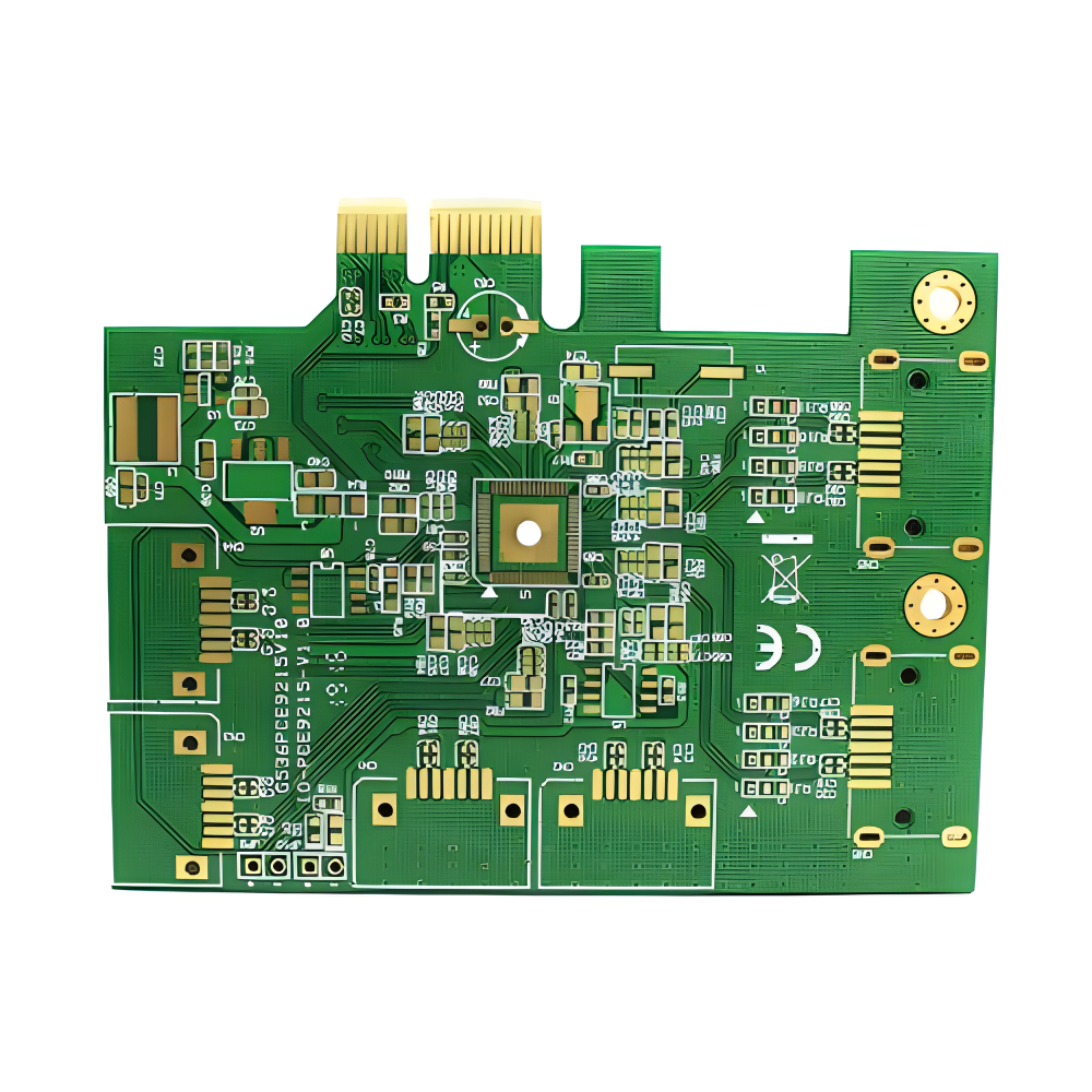 PTFE Teflon High-Frequency Board
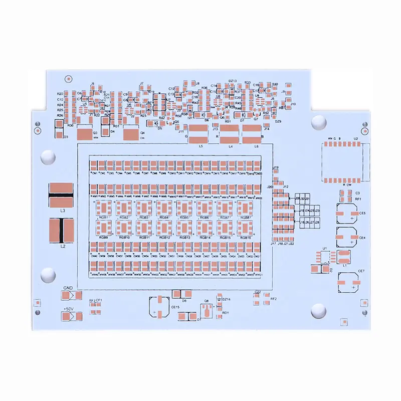 Aluminum
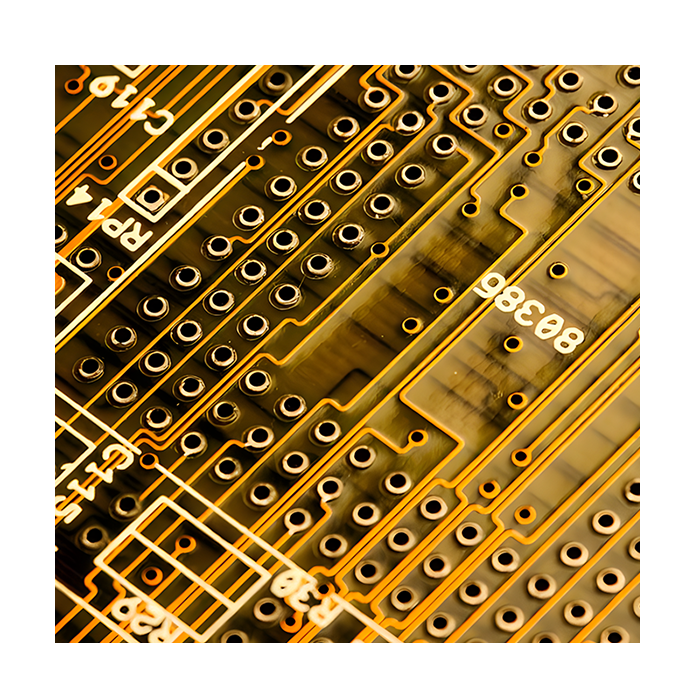 Copper Core
 PCB Assembly
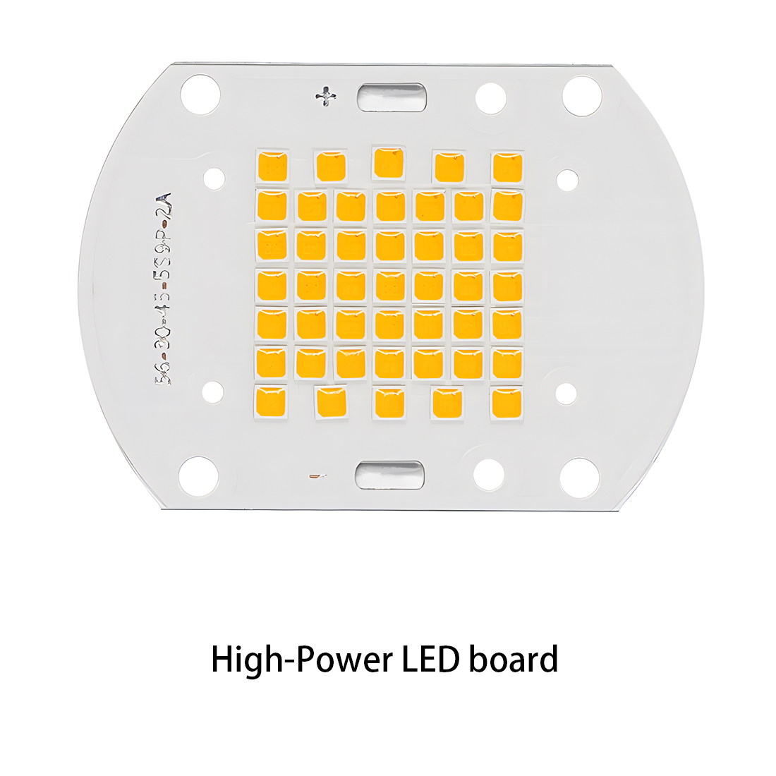 LED light PCBA
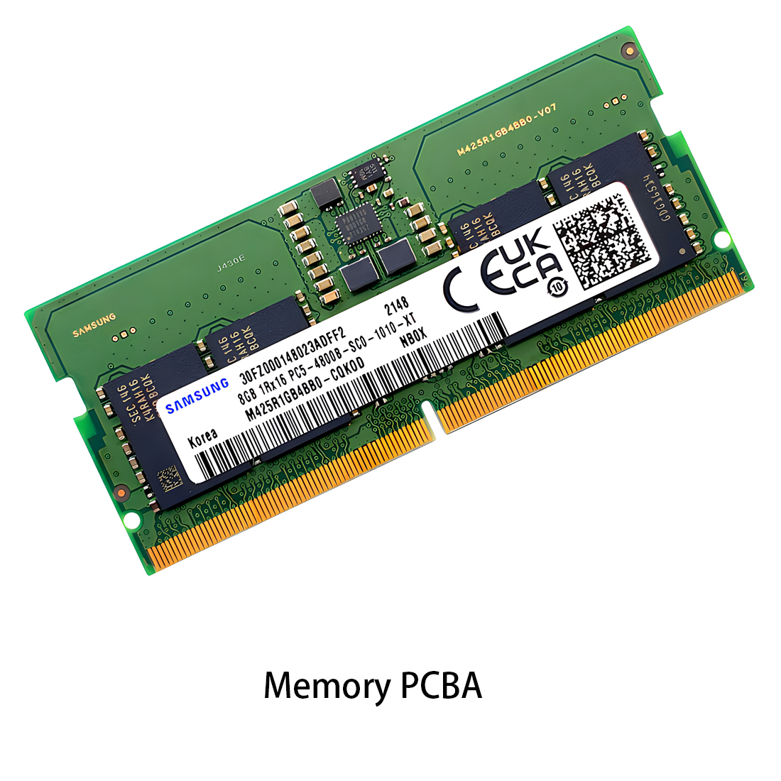 Memory PCBA
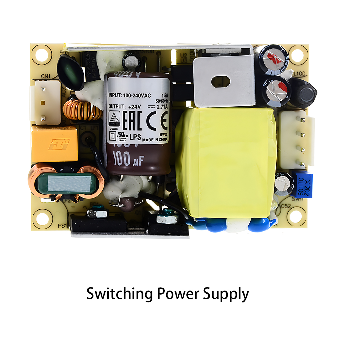 Power Supply PCBA
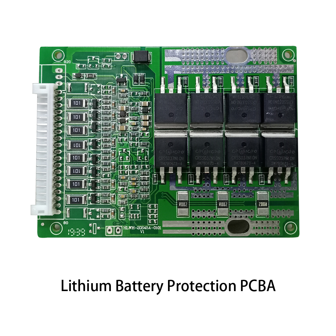 New Energey PCBA
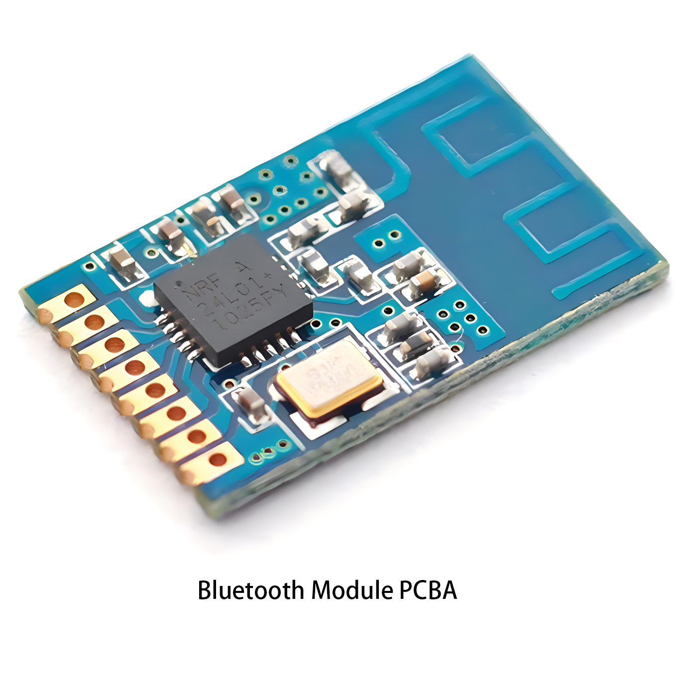 Communication PCBA
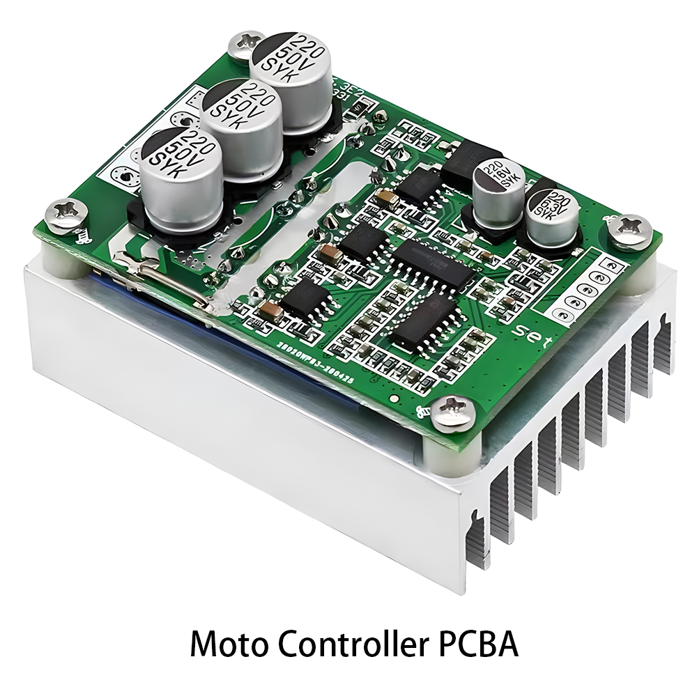 Industrial Control PCBA
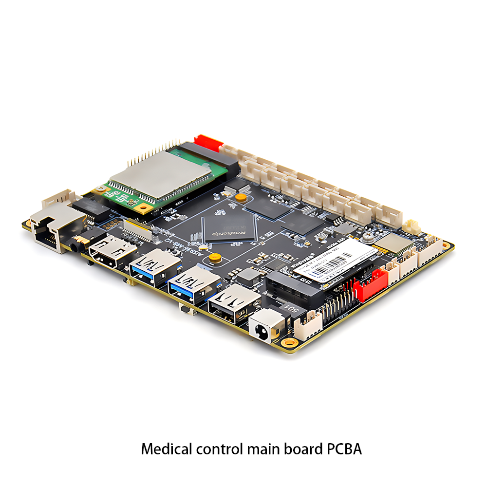 Medical Equipment PCBA
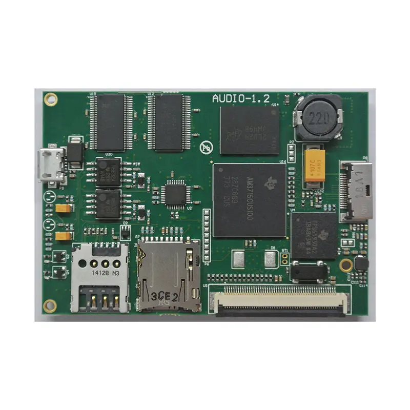 Testing Service
 PCBA Testing Service
 Certification Application
 RoHS Certification Application
 REACH Certification Application
 CE Certification Application
 FCC Certification Application
 CQC Certification Application
 UL Certification Application
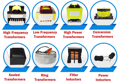 Transformers
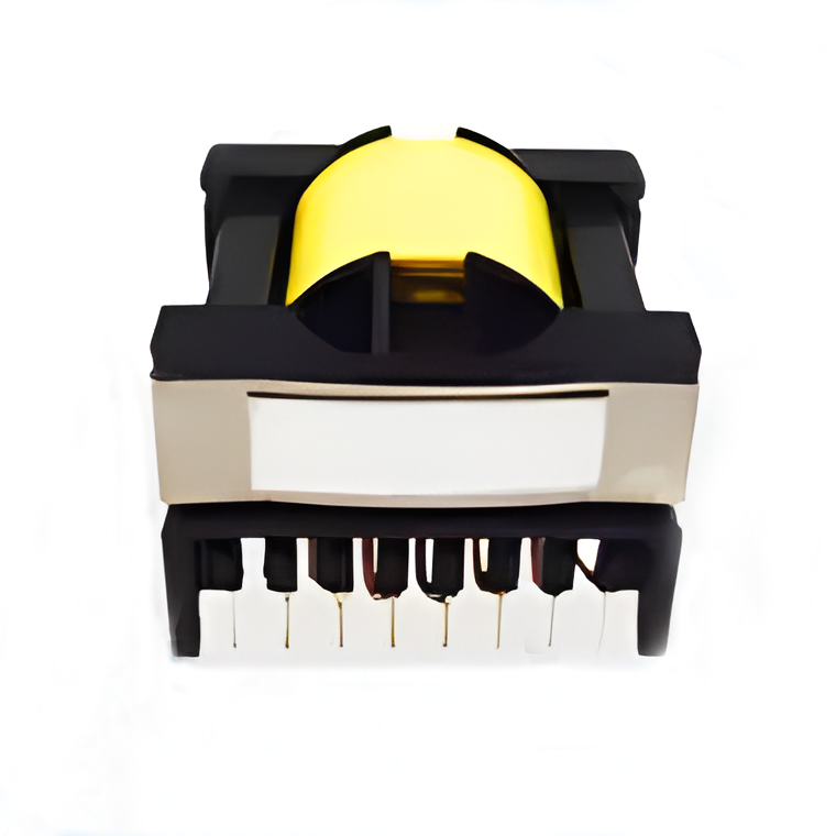 High Frequency Transformers
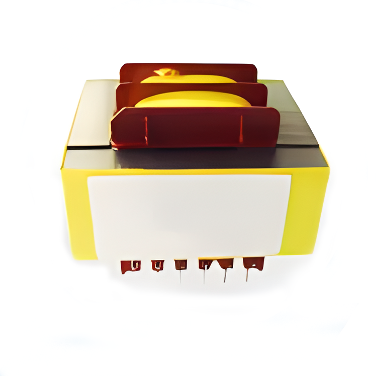 Low Frequency Transformers
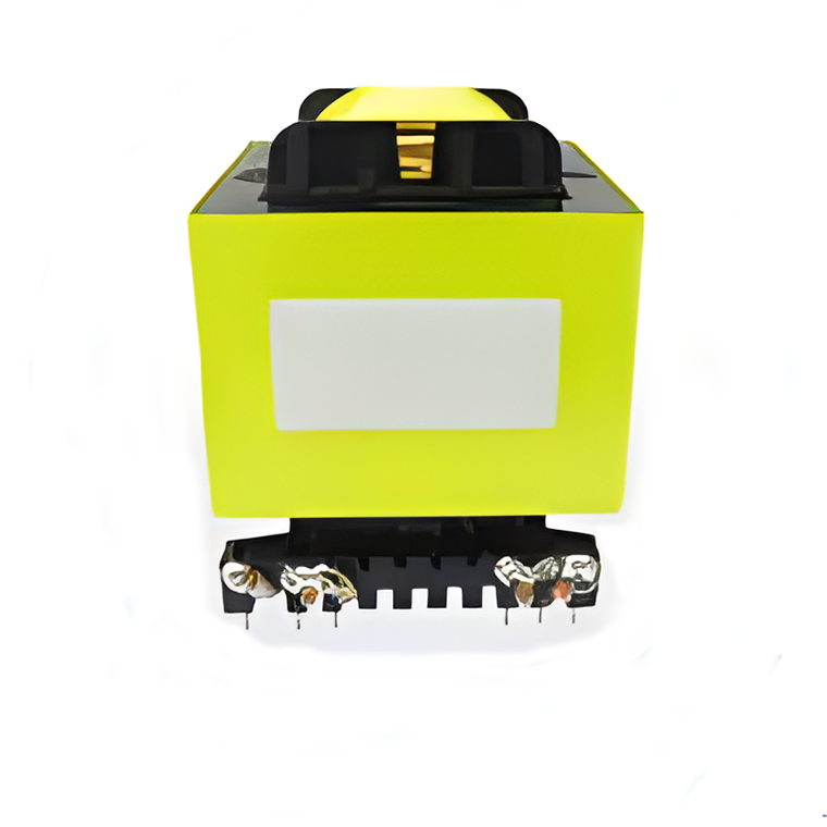 High Power Transformers
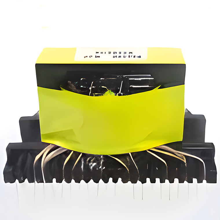 Conversion Transformers
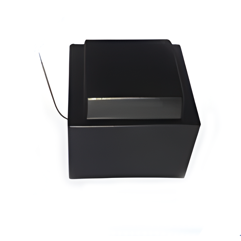 Sealed Transformers
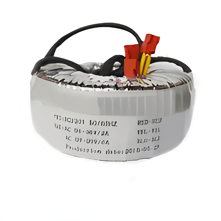 Ring Transformers
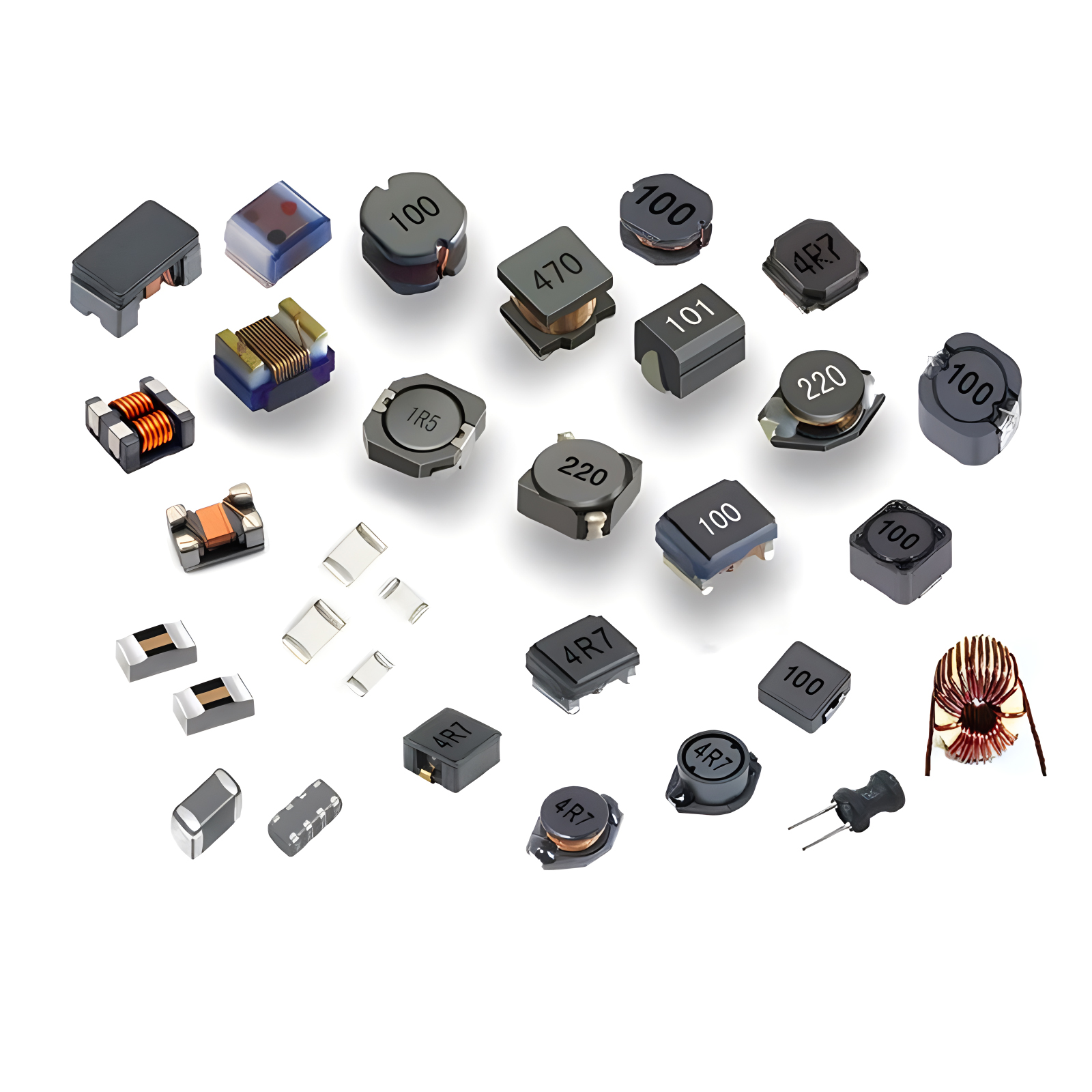 Inductors
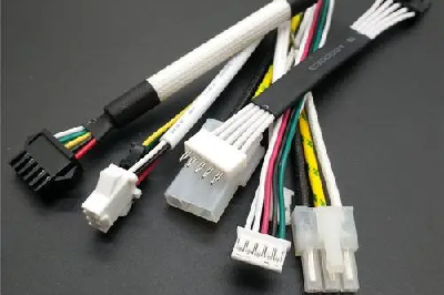 Wires,Cables Customized
 wires-cables

FR-4 PCB
An FR-4 PCB refers to a Printed Circuit Board (PCB) that uses FR-4 material as its substrate. FR-4 is a very common composite material used in PCB manufacturing. Its full name is Flame Retardant 4, indicating it meets a specific flame retardancy rating. This material consists of woven fiberglass cloth impregnated with epoxy resin, offering good electrical insulation properties, mechanical strength, and flame retardancy.
Here are some key characteristics of an FR-4 PCB:
● Flame Retardancy
● Electrical Performance
● Mechanical Strength
● Thermal Performance
● Cost-effectiveness
| No. | Item | Manufacturing Capabilities |
|---|---|---|
| 1 | Material | FR-4 (Fiberglass) |
| 2 | Number of Layers | 1 Layer, 2 Layers, 4 Layers, 6 Layer, 8 Layers,10 Layers
|
| 3 | TG Grade | TG130~140, TG150~160, TG170~180 |
| 4 | Max PCB Size |
1 layer & 2 layers: 1200*300mm or 600*500mm
Multi-layers: 600*500mm
|
| 5 | Min PCB Size | 5mm*5mm |
| 6 | Board Size Tolerance(Outline) |
±0.2mm(CNC routing)
±0.5mm(V-scoring)
|
| 7 | Surface Finish | HASL with lead, HASL lead free, Immersion gold(ENIG), OSP, Hard gold, ENEPIG, Immersion silver (Ag), None |
| 8 | Board Thickness |
1 Layer/2 Layers: 0.2~2.4mm
4 Layers: 0.4~2.4mm
6 Layers: 0.8~2.4mm
8 Layers: 1.0~2.4mm
10 Layers: 1.2~2.4mm
Note: Customized PCB thickness and Layer stackup are acceptable.
|
| 9 | Board Thickness Tolerance |
Thickness≥1.0mm: ±10%
Thickness<1.0mm: ±0.1mm
Note: Normally “+ Tolerance” will occur due to PCB processing steps such as electroless copper, solder mask and other types of finish on the surface.
|
| 10 | Outer Layer Copper Thickness |
1oz/2oz/3oz
(35μm/70μm/105μm)
Note:
2oz
PCB thickness≥1.2mm,Via Size≥0.25mm,Min Track/Spacing≥0.15mm
3oz
PCB thickness≥2.0mm,Via Size≥0.3mm,Min Track/Spacing≥0.2mm
|
| 11 | Inner Layer Copper Thickness |
1oz/1.5oz
(35μm/50μm)
|
| 12 | Outer layer Min track/spacing | ≥3mil |
| 13 | Inner layer Min track/spacing | ≥4mil |
| 14 | Annular Ring Size | ≥0.13mm |
| 15 | Grid Line track/spacing | ≥0.2mm |
| 16 | Coil board Line track/spacing | ≥0.2mm |
| 17 |
BGA pad size |
≥0.25mm |
| 18 | BGA Distance | ≥0.12mm |
| 19 | Board Outlines |
Track to Outline: ≥0.3mm
Trace to V-cut line: ≥0.4mm
|
| 20 | Finished Hole Size Tolerance | ±0.08mm |
| 21 | Finished Hole Diameter(CNC) |
0.2mm~6.3mm
1. PCB Thickness=2.0mm, Min Hole Size Is 0.3mm
2. PCB Thickness=2.4mm, Min Hole Size Is 0.4mm
3. Copper Thickness=2OZ, Min Hole Size Is 0.25mm
4. Copper Thickness=3OZ, Min Hole Size Is 0.3mm
|
| 22 | TH Via Distance |
Same nets: 0.15mm
Different net: 0.25mm
|
| 23 | Plated Slot Size |
≥0.5mm
Note:
L:W=2.5: 1 (Should be 2.5:1 or Higher. If It Is Less Than This, The Holes May Be Misaligned.) If You Can't Draw A Long Hole In Your Design, You Can Draw A Continuous Round Hole And It Will Be Regarded As A Long Hole. Also, It Is Okay To Draw The Oblong Hole In Profile Layer Instead Of Drilling Layer.
|
| 24 | Castellated Holes |
≥0.6mm |
| 25 | Non-Plated Holes | ≥0.8mm |
| 26 | NPTH to Copper Line | ≥0.2mm |
| 27 | Soldermask | Green, Red, Yellow, White, Black, Blue, Purple, Matte Green,Matte Black,None |
| 28 | Soldermask Thickness | 20~30um |
| 29 | Soldermask Bridge |
Green: ≥0.1mm
Others: ≥0.15mm
|
| 30 | Soldermask to soldering pad distance | ≥0.05mm |
| 31 | Silkscreen | White, Black, Yellow, None |
| 32 | Minimum Character Width(Legend) |
≥0.15mm
Note: Characters of less than 0.15mm wide will be too narrow to be identifiable.
|
| 33 | Minimum Character Height (Legend) |
≥0.75mm
Note: Characters of less than 0.8mm high will be too small to be recognizable.
|
| 34 | Character Width to Height Ratio (Legend) | 1: 5 (In PCB silkscreen legends processing, 1:5 is the most suitable ratio) |
| 35 | Silkscreen to Soldering Pad Distance | ≥0.1mm |
| 36 | V-cut Line |
≥70mm
Note:
PCB thickness≥0.6mm
|
| 37 | V-cut Line Distance | ≥3.5mm |
| 38 | Distance betwen Board to Board | ≥0.8mm |
| 39 | Stamp-hole Width |
≥2.0mm
Note: PCB size and thickness are subject to review by Minintel.
|
| 40 | Tab-route Width |
≥1.6mm
Note: PCB size and thickness are subject to review by Minintel.
|
| 41 | Edge Rail |
≥3.5mm
Note: If the pannels are arrayed by Minintel, we will add 5mm edge rails on both sides by default.
|
| 42 | Gold Finger |
Bevelling Angle: 30~45°
Depth: ≥1mm
Length: 45mm~280mm
Note: Board thickness≥1.2mm
|
| 43 | Special Specification |
Impedance control
Custom Layer Stackup
Interstitial Via Hole(IVH)
Via in pad
Via filled with resin
Countersinks/Counterbores
Carbon Mask
Halogen-Free
Z-axis milling
Edge Plating
Others
|
submit now