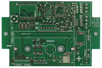
 PCB
PCB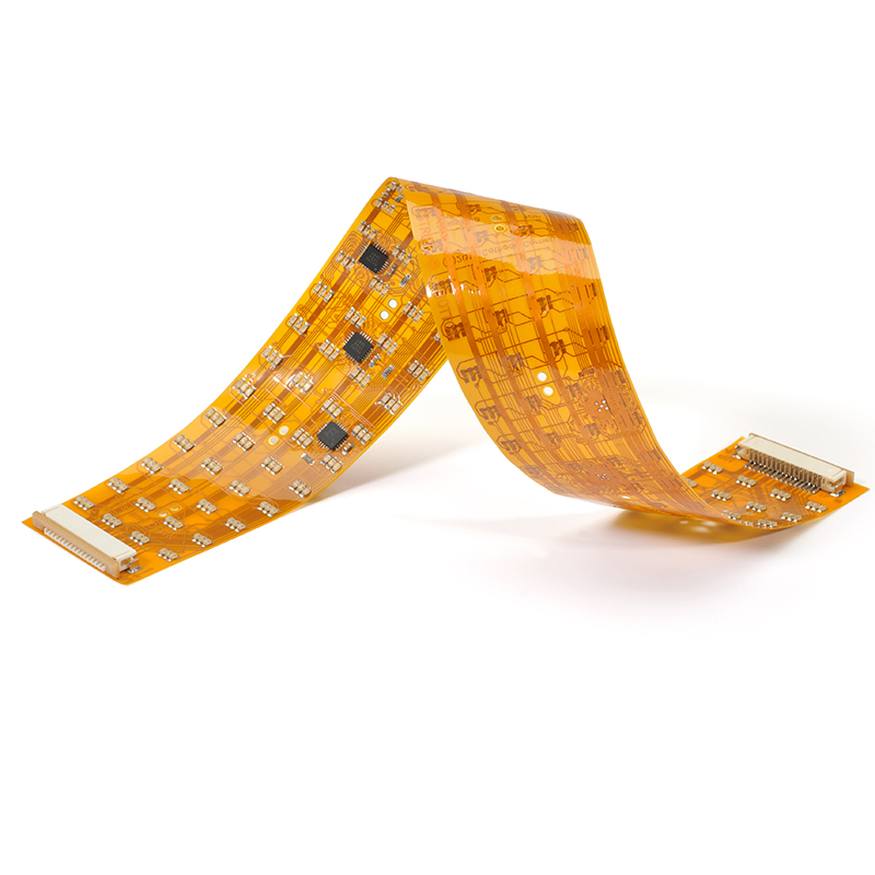 FPC
FPC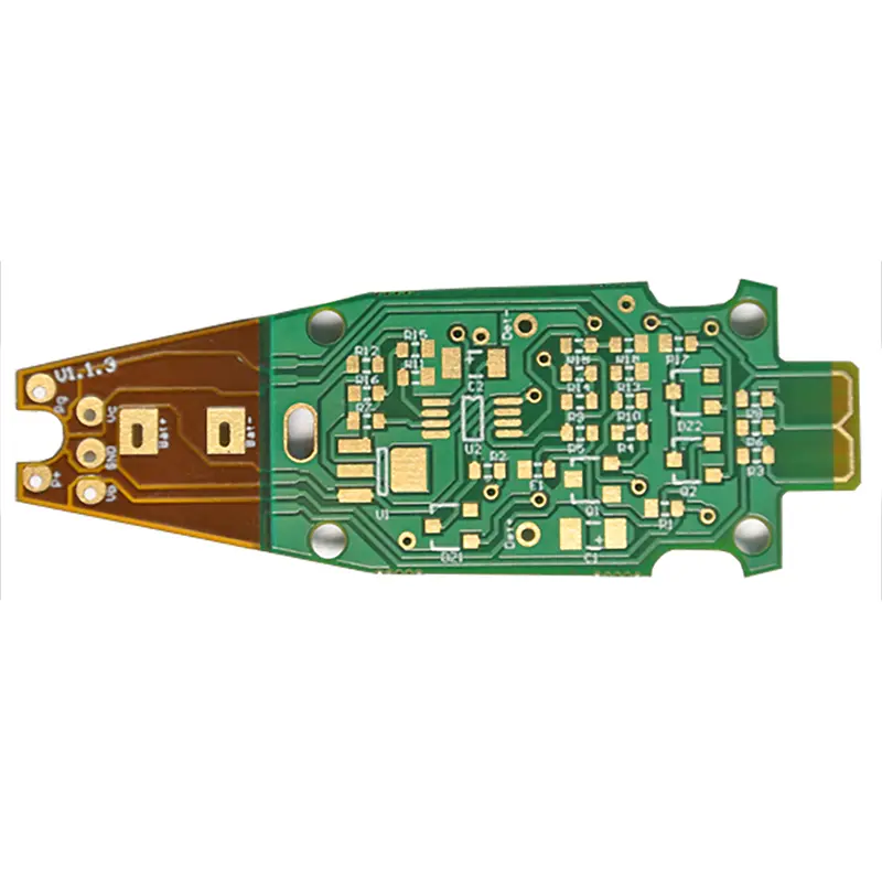 Rigid-Flex
 FR-4
FR-4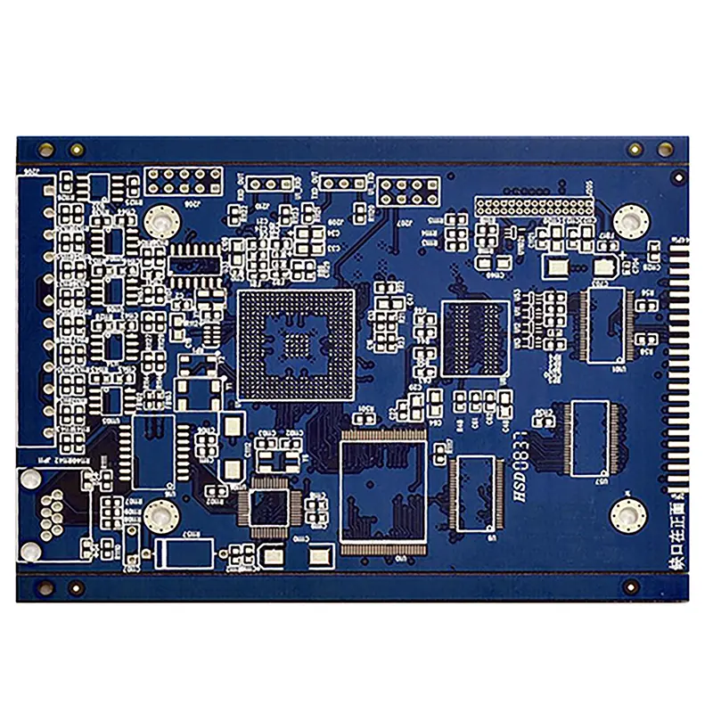 HDI PCB
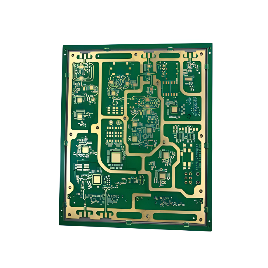 Rogers High-Frequency Board
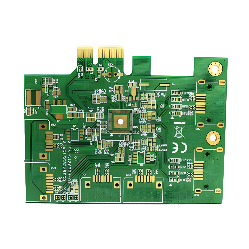 PTFE Teflon High-Frequency Board
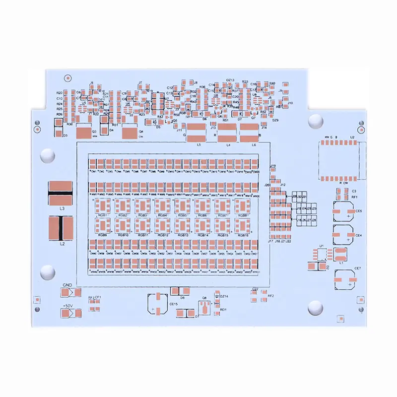 Aluminum
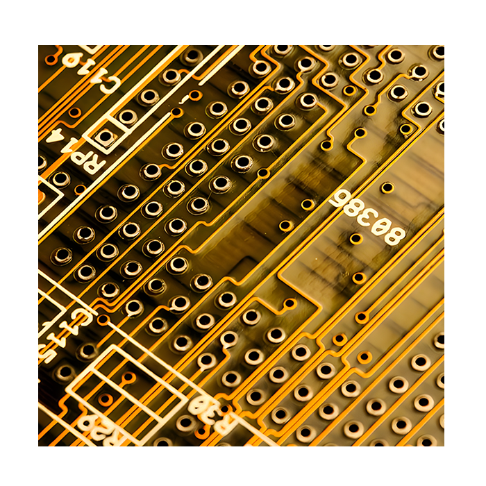 Copper Core
 PCB Assembly
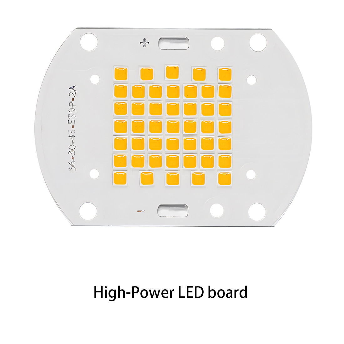 LED light PCBA
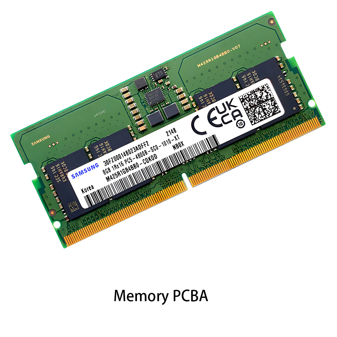 Memory PCBA
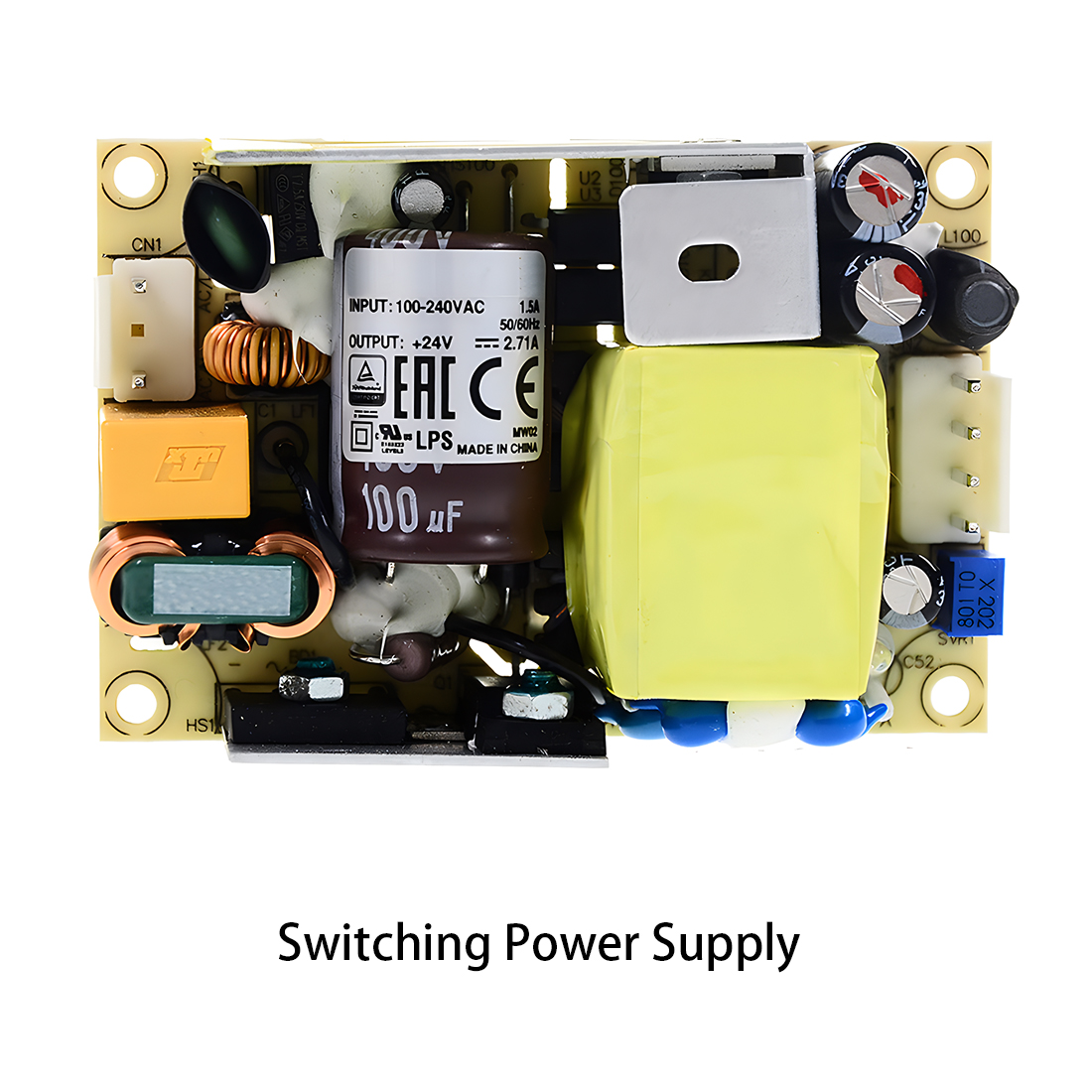 Power Supply PCBA
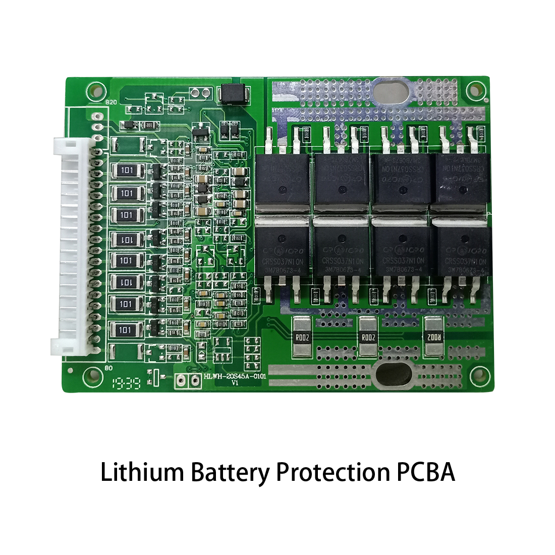 New Energey PCBA
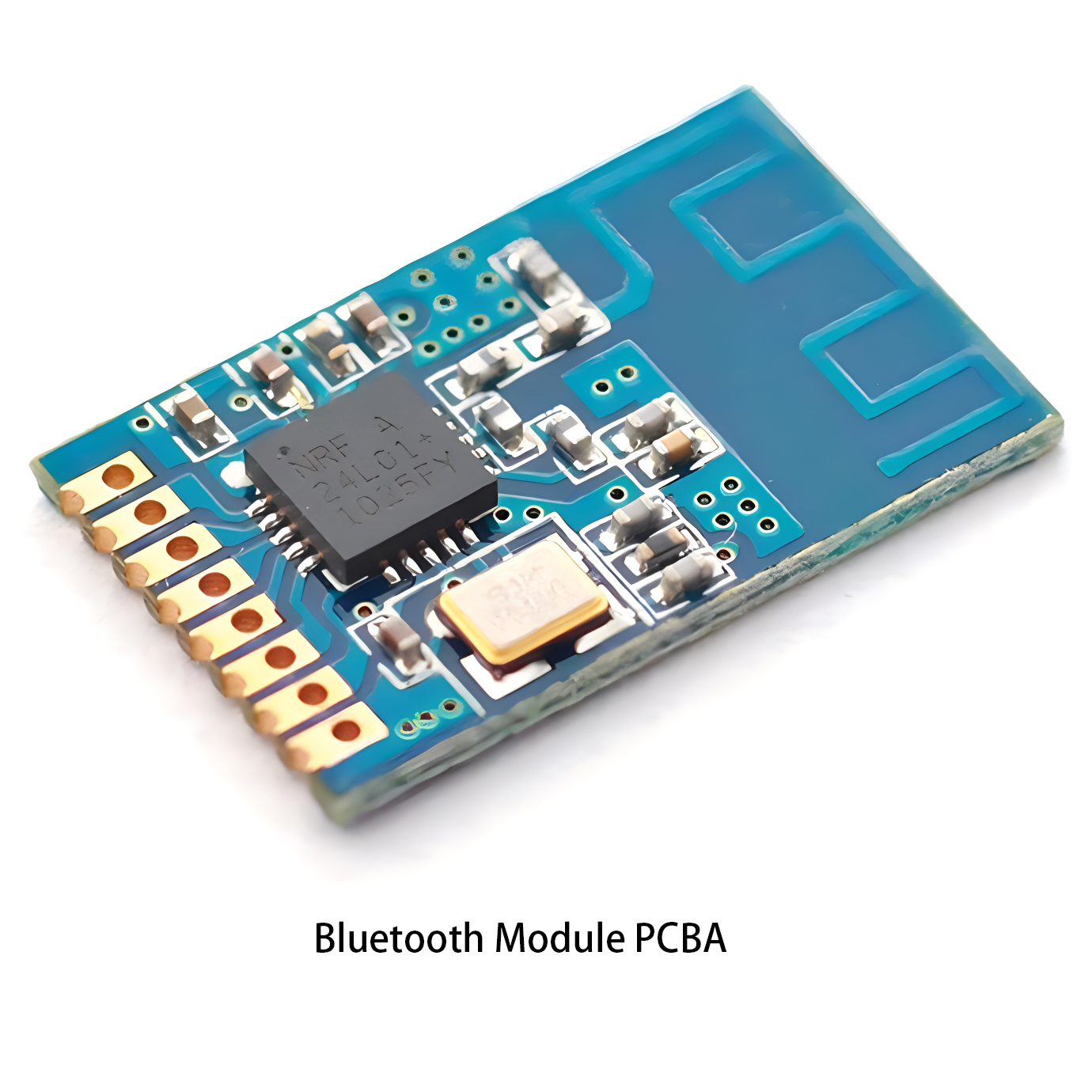 Communication PCBA
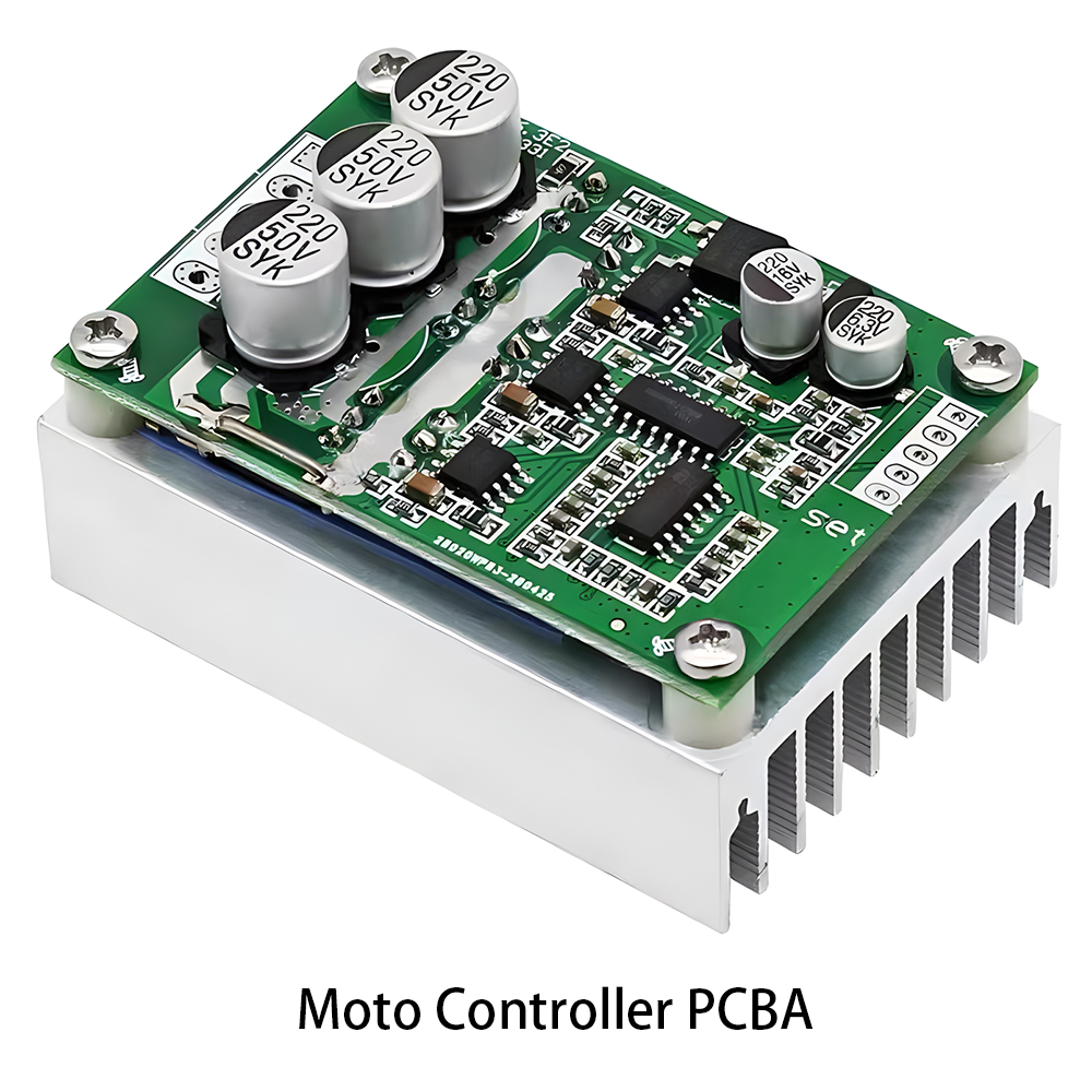 Industrial Control PCBA
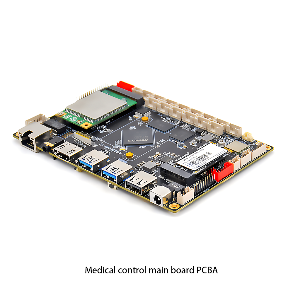 Medical Equipment PCBA
 Testing Service
 PCBA Testing Service
 Certification Application
 RoHS Certification Application
 REACH Certification Application
 CE Certification Application
 FCC Certification Application
 CQC Certification Application
 UL Certification Application
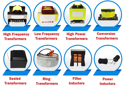 Transformers
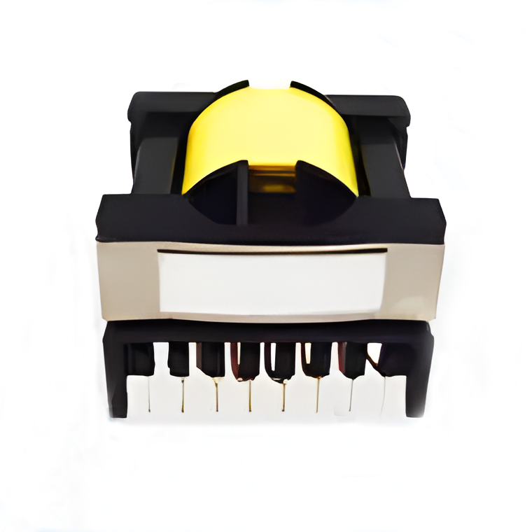 High Frequency Transformers
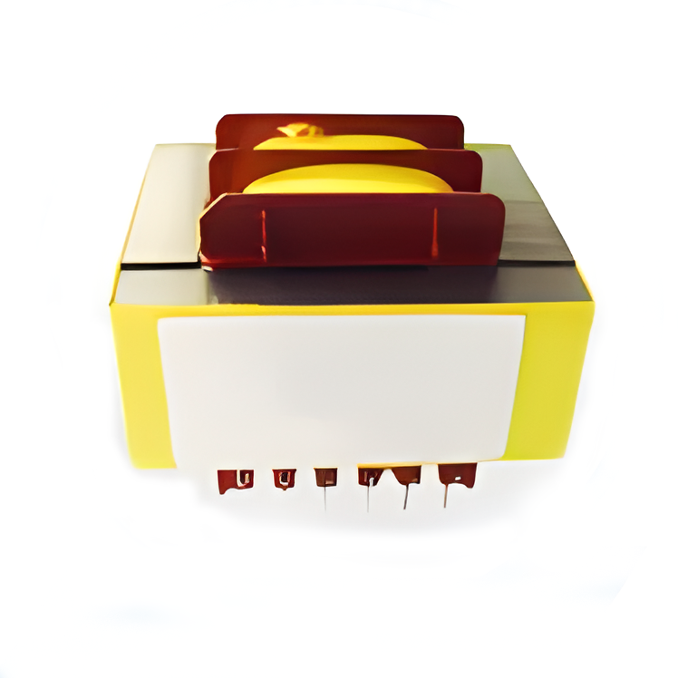 Low Frequency Transformers
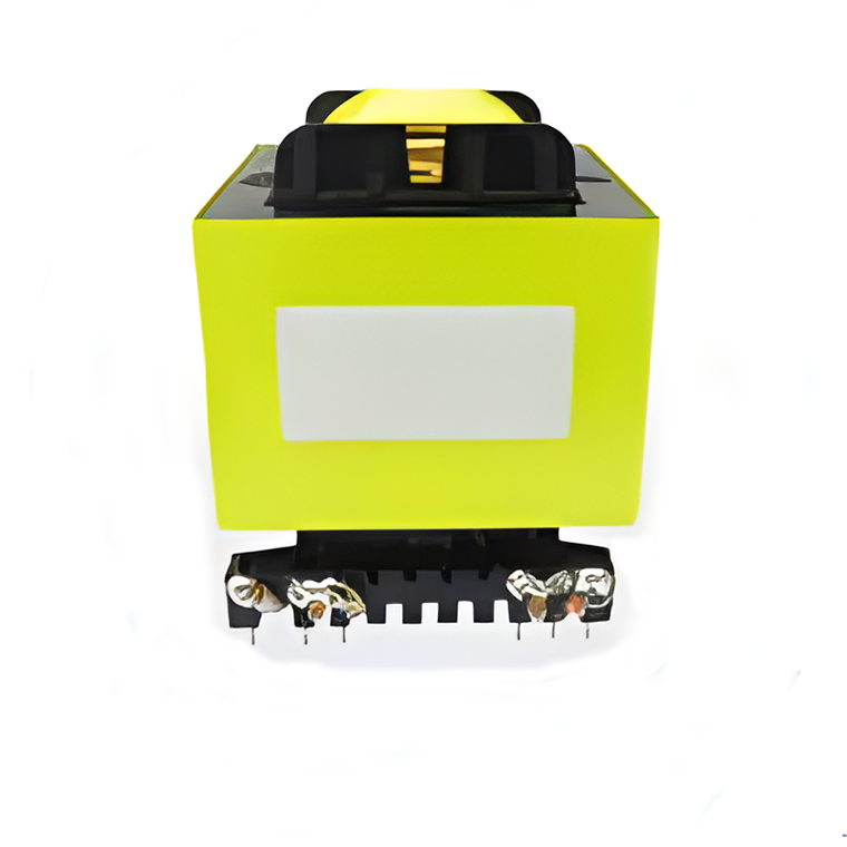 High Power Transformers
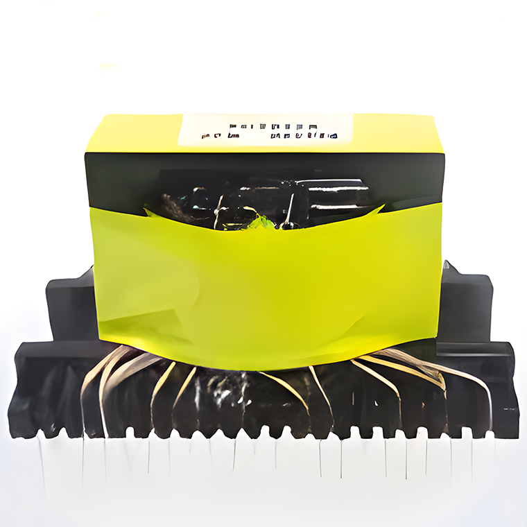 Conversion Transformers
 Sealed Transformers
 Ring Transformers
 Inductors
 Wires,Cables Customized
 wires-cables
One type PCB defect caused by bad solder mask
2024-03-13 02:08:00
We can see from below figure that there are 13 vias inside the footprint of the MCU on the PCB, and there is a large pad at the bottom of the MCU that connects to GND.
If the solder mask layer is not thick enough, the copper of some vias will not be covered by the solder mask ink, when the MCU is assembled by the SMT machine, the big pad of MCU will short with the vias, it will cause a disaster in the production.
![H]}T8)VNH%784X5(@%]QIUJ.png](https://ecdn6.globalso.com/upload/p/76/image_other/2024-03/65f094ae0d76347932.png)
How can we avoid this type defect?
- When we design the PCB, if we find there is a big bare pad under the chips, we should not place the vias or wires under this pad;
- If we must place the vias under the bare pad of the chips, we should find a good PCB manufacturer who can process enough thickness solder mask to keep opening circuit between the vias and bare pad.
Our company can manufacture high quanlity PCB to avoid this kind defect, and we also can provide the PCB design suggestion for customer.
A good PCB design will be helpful for mass productions.