You know, in the fast-changing world of electronICs, getting a good handle on Pcb Board Design is pretty much a must for engineers and manufacturers aiming for the top. I recently came across a report from MarketsandMarkets that said the global PCB market could hit around $85 billion by 2025. That just shows how important smart design and assembly are to keep up with the crazy demand for new gadgets.
Companies like Minintel Technology Co., Ltd. and Mingying Technology Co., Ltd. are really key players here—they’re leading the way as top PCBA makers and offering cutting-edge solutions to their customers. Knowing the ins and outs of PCB Board Design isn’t just about making products work better, it also helps speed up manufacturing and cut down costs. Ultimately, it’s about hitting those targets in a pretty competitive space. In this guide, I’ll share some handy tips and techniques that can help engineers and manufacturers refine their design game and get better results on their projects.
Understanding the Fundamentals of PCB Design: Key Concepts and Terminology
When you're diving into Pcb Design, it’s really important to get a solid grasp of the basics and the key terminology. I mean, understanding terms like 'trace width,' 'via,' and 'ground plane' isn’t just nerdy stuff—it's essential for clear communication and doing good work. Oh, and did you hear about the latest update? The sixth edition of IEC 60194:2015 has come out, bringing fresh standards that help guide us through making and assembling printed circuit boards. Sticking to these industry rules not only keeps you compliant but also boosts the overall quality and reliability of your PCBs.
If you’re serious about getting better at PCB design, a few tips might help. For starters, really get comfortable with those core terms I mentioned earlier—they’re the foundation of your discussions and planning. Also, don’t shy away from new tech, like ultra high-density interconnects (UHDI). These are pretty cool—they allow for lines and spaces smaller than 25 microns, which is perfect if you’re aiming for super compact, efficient devices.
And here’s a bonus tip: tap into collaborative resources. Reading columns or insights from industry pros can spark fresh ideas and help you tackle tricky design challenges. Keep yourself in the loop, keep learning, and you’ll find that navigating this fast-changing field gets a lot easier—and maybe even kinda fun!
The Importance of Key Concepts in PCB Design
Essential Software Tools for PCB Design: Choosing the Right Solutions
When you're diving into PCB design, picking the right software can really make or break your workflow—and let's be honest, no one wants to get bogged down with clunky tools. The market’s pretty crowded, so it’s important to consider options that fit your specific needs, especially when it comes to prototyping. The right software can boost your productivity and even spark some fresh ideas, so taking the time to evaluate features thoroughly is definitely worth it. I’d suggest looking for something with an intuitive interface, solid features, and a supportive community that can help you troubleshoot when things get tricky.
A good rule of thumb? Focus on what’s a good fit for your project. Think about the complexity of your boards—are they simple or really intricate? Do you need any special functions? Also, don’t forget about support resources. Easy access to tutorials and help guides can make learning the software way less stressful. And hey, try out free demo versions whenever you can before going all in. It’s the best way to see if it meshes well with your workflow.
Staying up-to-date with the latest in PCB design tools is also a smart move. Many platforms keep adding new tech to help you design more accurately and faster. By keeping an eye on current trends and updates, you’ll be in a better position to pick features that truly help you work smarter. In a nutshell, doing your homework now can really pay off and keep you ahead of the game.
Design Best Practices: Tips for Creating High-Performance PCBs
In today’s fast-changing world of electronics, getting a good grip on PCB design is more important than ever if you wanna achieve top-notch performance. Mixing high-speed digital signals with high-frequency RF components has become a pretty big deal lately. I read a recent report that pointed out how tricky it’s getting to keep signals clean, especially with all the surge in IoT devices and other sleek wireless tech. When designing PCBs, you really gotta think about layout and routing carefully to prevent signal degradation — it’s all about safeguarding signal quality in complex setups.

Thanks to AI-powered tools now making waves in PCB design, things are changing quickly. Engineers are jumping on web-based platforms that let them collaborate in real time, making the whole process way more accurate. Apparently, using these AI layout tools can cut down design time a lot and make manufacturing smoother. Following best practices like keeping proper spacing and having solid ground planes is still super important — they’re basic but critical. Looking ahead to 2025, jumping on these new tech trends isn’t just a good idea, it’s pretty much essential if you want your projects to stand out and perform at their best.
Troubleshooting Common PCB Design Mistakes: How to Avoid Costly Errors
When you're designing a printed circuit board (or PCB for short), it's super important to avoid those common mistakes that can really mess things up, both in terms of how well it works and how much it costs. One of the biggest rookie errors? Not paying enough attention to component placement. If everything’s a mess and everything is scattered around, it can cause issues like poor signal quality and more electromagnetic interference. To keep that in check, I always recommend sketching out your layout early on. Think about the signal flow and try to keep interconnected parts close together—that makes a huge difference. Using a detailed Bill of Materials (or BOM) can also really streamline things, making sure you’ve got all the right parts in the right spots from the start.
Another common slip-up is forgetting about thermal management. Overheating can happen when high-power components are placed too close to sensitive areas. Not planning for proper heat dissipation can lead to components failing or performance dropping. Things like thermal vias and keeping enough space between heat-generating parts and fragile circuits are must-dos. And if you can, running thermal simulations during the design phase can help spot potential hot spots before you even send the board off for manufacturing. By catching these issues early, you save yourself from costly headaches down the line—and your design will turn out way better in the end.

Advanced Techniques for PCB Layout: Optimizing Signal Integrity and Power Distribution
When it comes to PCB design, getting a good handle on advanced layout techniques is a total game-changer. It’s super important for keeping signals clean and making sure power gets distributed smoothly. At Minintel Technology Co., Ltd., we totally get how vital these factors are for building top-notch PCBA solutions. By blending a bit of art with science in PCB design, engineers can better dodge issues like electromagnetic interference and make sure power flows quickly and evenly across the board.
One tip I’d toss out for boosting signal integrity is to keep the critical signal traces as short as you can. This usually means strategically placing your components and routing your traces carefully—avoiding tricky bends and loops that can cause unwanted inductance or capacitance. And don’t forget about ground planes—they serve as a solid reference point for signals, helping cut down noise and bumping up overall performance.
Another thing that really helps is paying close attention to power distribution. Making power traces wide enough to handle the current prevents voltage drops and stops things from overheating. Plus, adding decoupling capacitors, placed as close as possible to the power pins, can smooth out voltage fluctuations and keep everything running steady. Following these practices, designers can create really robust PCBs that meet the high demands of today’s advanced electronics out there.
The Definitive Ultimate Guide to Mastering PCB Board Design: Tips and Techniques for Success
| Design Aspect | Technique | Benefits | Challenges |
| Signal Integrity | Differential Pair Routing | Reduces noise and crosstalk. | Requires careful trace length matching. |
| Power Distribution | Ground Plane Design | Improves power integrity and EMI performance. | Increases board size if not accounted for early. |
| Thermal Management | Thermal Via Placement | Helps dissipate heat away from components. | Requires precise calculation of thermal paths. |
| EMI Reduction | Shielding Techniques | Minimizes electromagnetic interference. | Can complicate assembly and layout. |
| Design DRC | Design Rule Check (DRC) | Ensures all design constraints are met. | False positives can lead to unnecessary changes. |
Prototyping and Testing Your PCB Design: Steps for Successful Validation
Prototyping and testing your PCB design are super important steps—you really want to make sure everything works just right before moving forward. According to a report by IPC, almost half of PCB design failures happen because of issues caught during the prototyping phase. That just shows how crucial it is to create prototypes that truly reflect what you’re aiming for in the final design. Using advanced tools like CAD software is a game-changer—it allows you to simulate different conditions, which helps spot potential problems early on. Doing this saves you a ton of time and money down the line on costly revisions.
Once you've built your prototype, testing becomes the next key step. Interestingly, a study from IEEE found that products that go through thorough testing before hitting the market tend to have about 30% fewer defects. It’s important to check both electrical and mechanical aspects to make sure your PCB can handle real-world use. And using automated testing tools? That can really speed things up, making it easier to make quick adjustments and use your resources wisely. All in all, focusing on solid prototyping and comprehensive testing leads to more reliable, successful PCB designs—and nobody wants to deal with avoidable issues after launch!
Innovative Solutions: A Comprehensive Guide to Wire To Board Connectors for Your Projects
In today's rapidly evolving electronics landscape, the importance of reliable wire-to-board connectors cannot be overstated. These components are vital in establishing robust connections between circuit boards while ensuring efficient signal transmission and power distribution. A recent industry report by MarketsandMarkets highlights that the global wire-to-board connector market is expected to grow from $4.9 billion in 2022 to $7.2 billion by 2027, reflecting a compound annual growth rate (CAGR) of 8.4%. This surge is driven by the increasing demand for compact and reliable electronic devices across sectors such as automotive, telecommunications, and consumer electronics.
Minintel is proud to be at the forefront of this industry by offering high-quality wire-to-board connectors sourced from renowned global manufacturers. Our rigorous supplier screening process ensures that only those who meet strict quality control standards are chosen, allowing us to promise excellence in performance and durability. Each product undergoes comprehensive testing, including electrical performance and environmental compatibility assessments, ensuring they are fit for the challenges presented by modern applications.
Furthermore, Minintel recognizes the need for competitive pricing, especially for businesses looking to scale. Our pricing strategies are designed to assist clients in reducing costs while maintaining quality, ensuring they remain competitive in an ever-changing market. As companies continue to innovate and push the boundaries of technology, partnering with a reliable supplier like Minintel is essential for achieving sustainable growth and success in electronic component procurement.
FAQS
: Neglecting proper component placement can lead to poor signal integrity and increased electromagnetic interference. It is important to plan the layout in advance to minimize distances between interconnected components.
A well-organized Bill of Materials (BOM) can enhance the design process by ensuring that all necessary components are accounted for and properly placed.
Proper thermal management is crucial to avoid heating issues that can lead to component failure and reduced performance. It is essential to ensure appropriate spacing between heat-generating components and sensitive circuits.
Employing thermal simulation tools during the design phase can help identify potential hot spots before the board is fabricated.
Prototyping is critical for validating and ensuring the functionality of the PCB design. It helps identify issues early in the process, significantly reducing the likelihood of costly revisions.
Products that undergo thorough testing before market release experience 30% lower defect rates, highlighting the importance of comprehensive evaluations in both electrical and mechanical aspects.
Automated testing solutions enhance efficiency during the testing stage by allowing rapid iterations and better utilization of resources.
Advanced CAD software enables designers to simulate various conditions, which helps identify potential problems early on, reducing the chances of design failures later.
The testing process should include both electrical and mechanical evaluations to ensure that the PCB can withstand real-world conditions.
By proactively addressing issues related to component placement and thermal management, and by focusing on effective prototyping and comprehensive testing, you can significantly reduce the likelihood of costly errors.

 Capacitors
 Connectors
 Diodes
 Embedded Processors & Controllers
 Communication Modules/IoT
 Resistors
 Switches
 Transistors
 Power Modules
 RF and Wireless
 PCB
 FPC
 Rigid-Flex
 FR-4
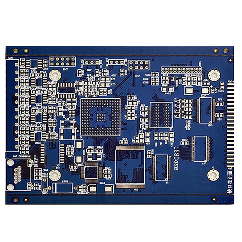 HDI PCB
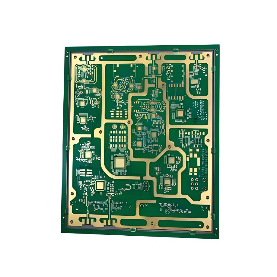 Rogers High-Frequency Board
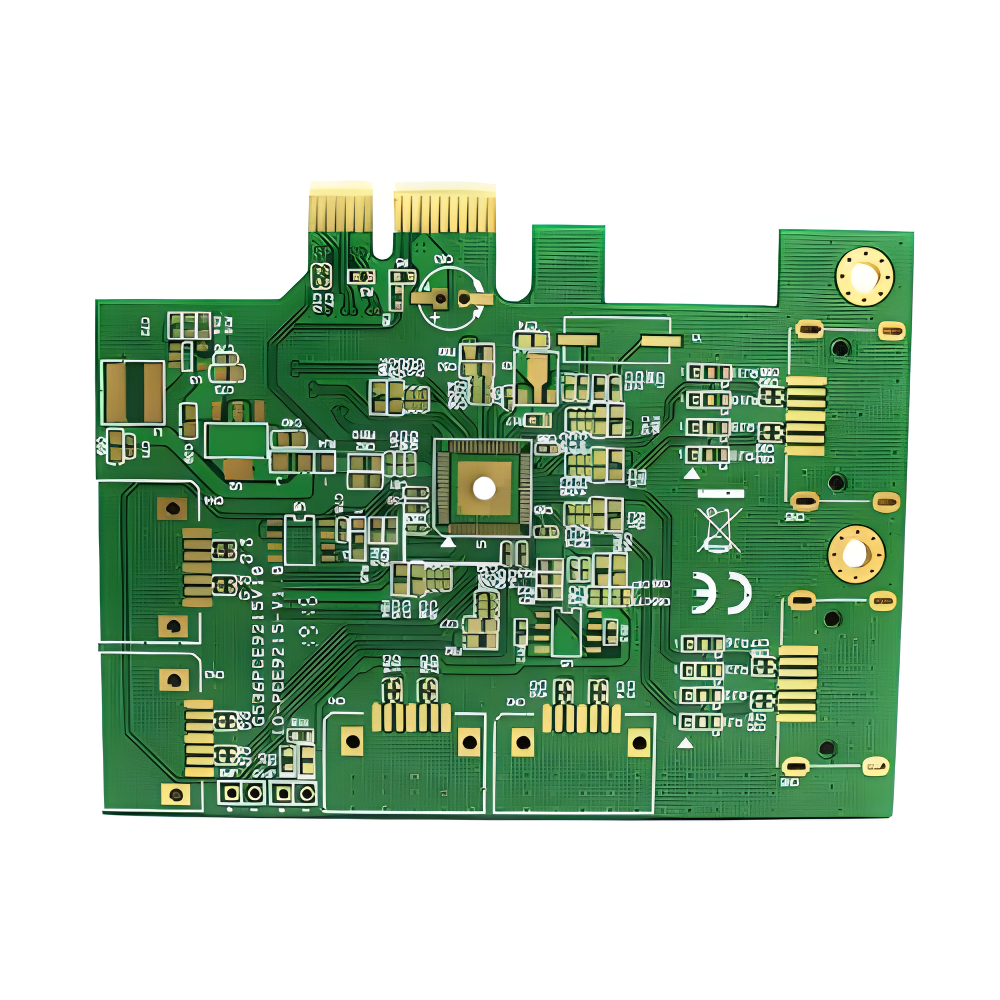 PTFE Teflon High-Frequency Board
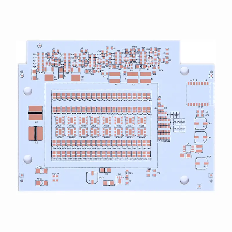 Aluminum
 Copper Core
 PCB Assembly
 LED light PCBA
 Memory PCBA
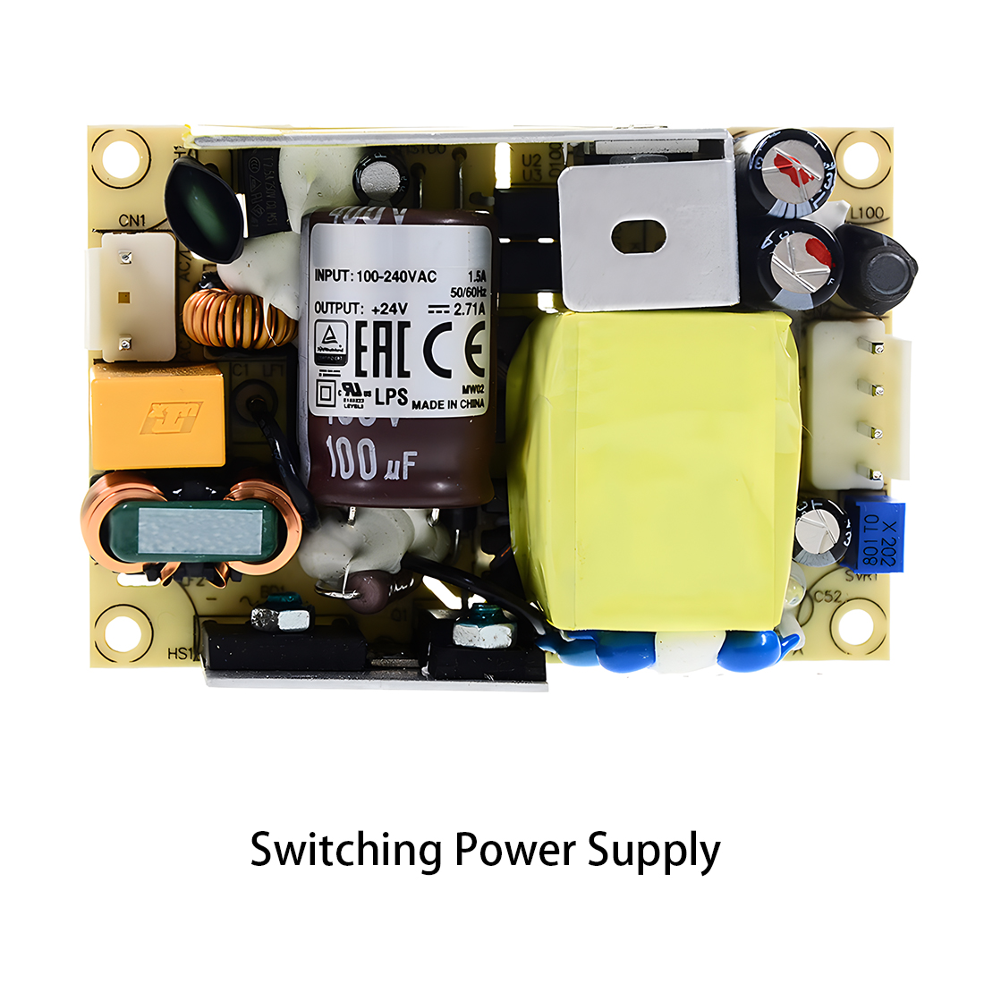 Power Supply PCBA
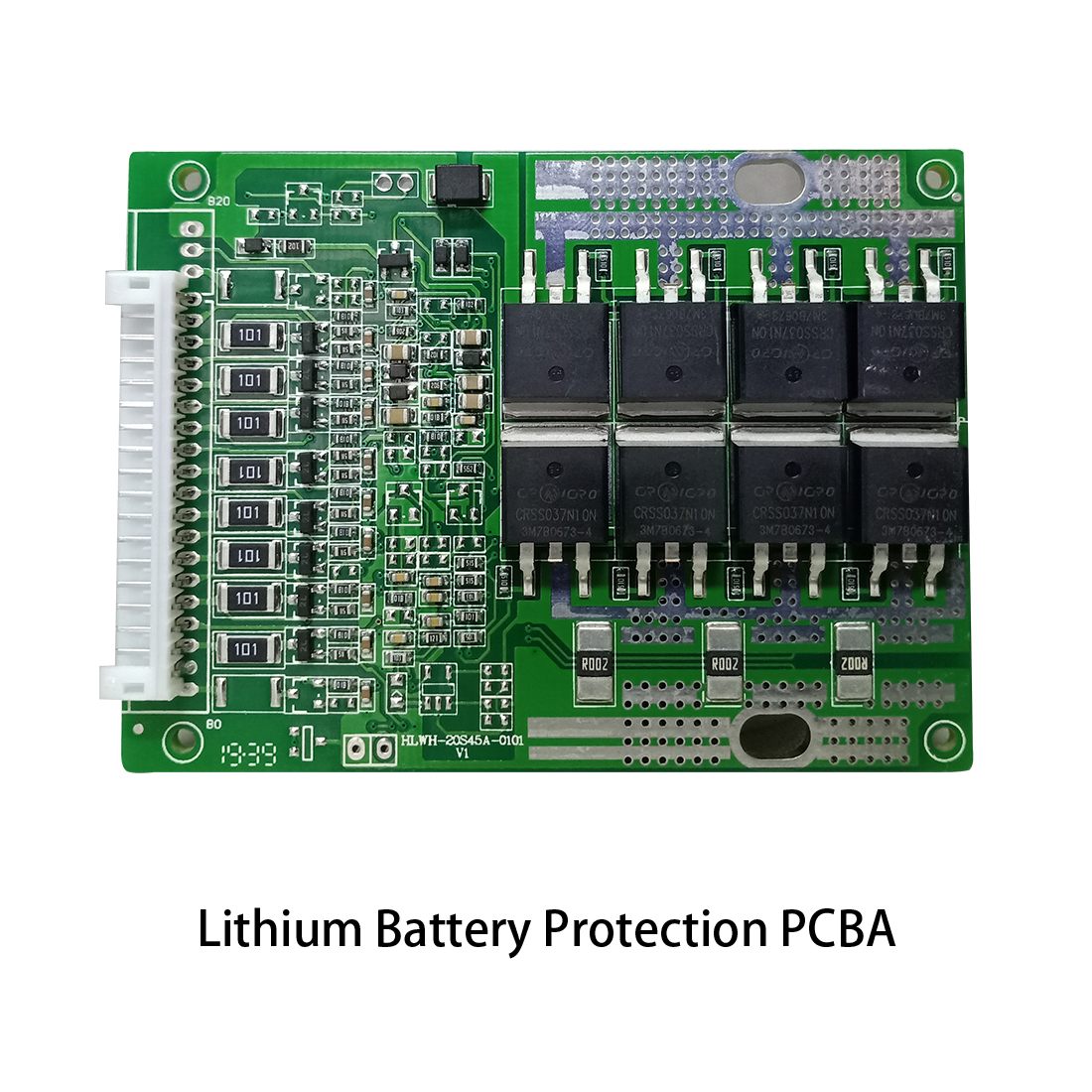 New Energey PCBA
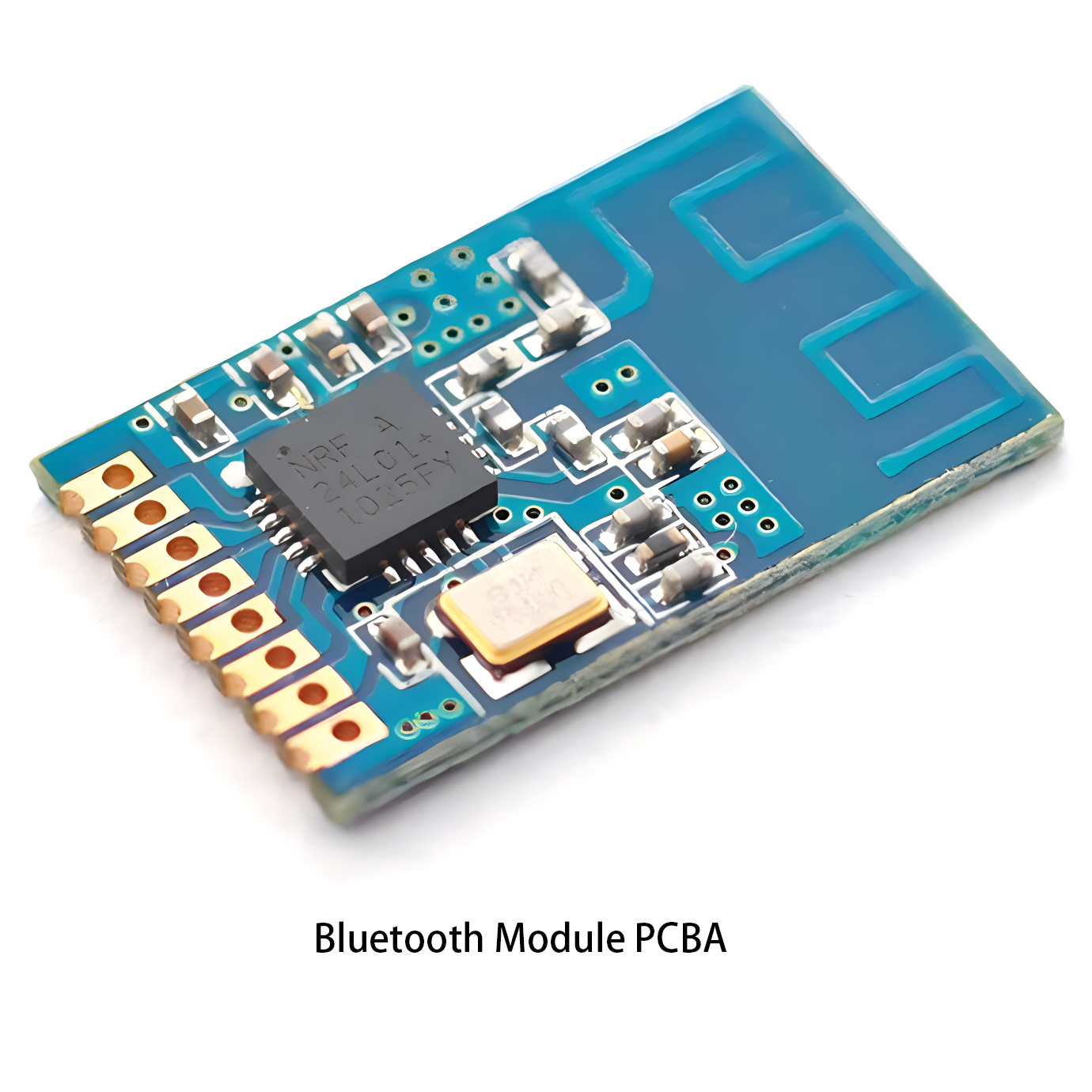 Communication PCBA
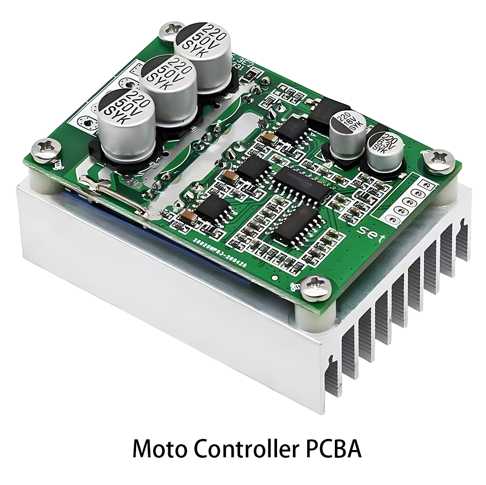 Industrial Control PCBA
 Medical Equipment PCBA
 Testing Service
 PCBA Testing Service
 Certification Application
 RoHS Certification Application
 REACH Certification Application
 CE Certification Application
 FCC Certification Application
 CQC Certification Application
 UL Certification Application
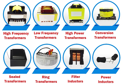 Transformers, Inductors
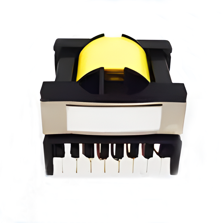 High Frequency Transformers
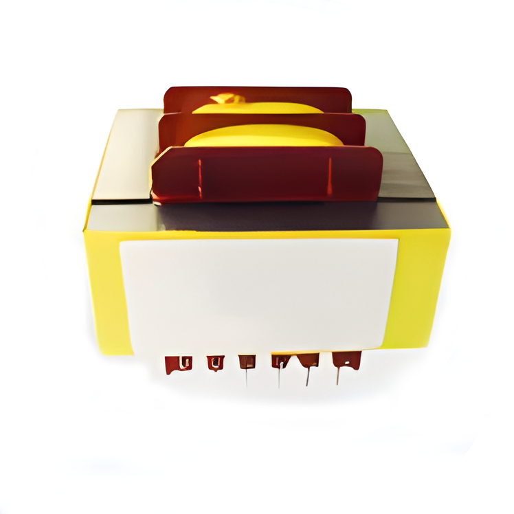 Low Frequency Transformers
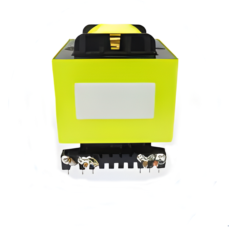 High Power Transformers
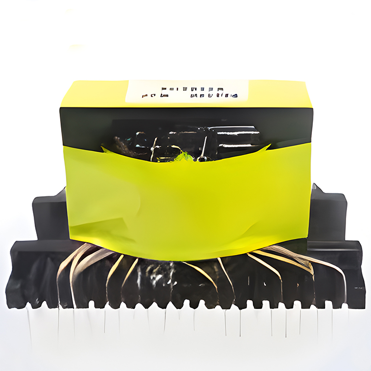 Conversion Transformers
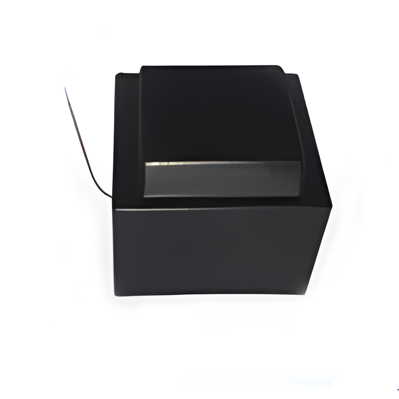 Sealed Transformers
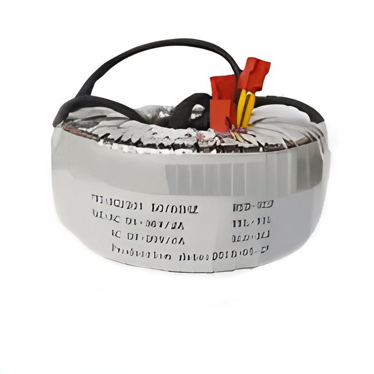 Ring Transformers
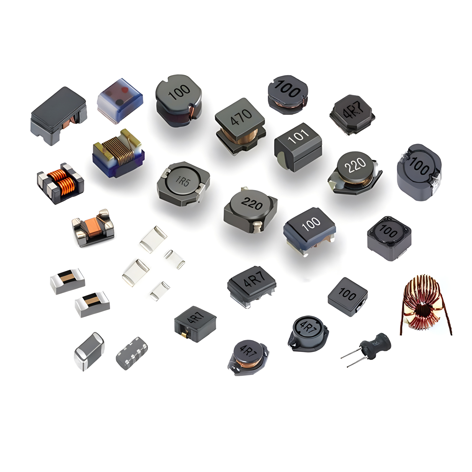 Inductors
 Wires,Cables Customized
 Network Cables
 Power Cords
 Antenna Cables
 Coaxial Cables
 Net Position Indicator
 Solar AIS net position indicator
 Digital Signal Processors (DSP/DSC)
 Microcontrollers (MCU/MPU/SOC)
 Programmable Logic Device(CPLD/FPGA)
 Through Hole Resistors
 Resistor Networks, Arrays
 Potentiometers,Variable Resistors
 Aluminum Case,Porcelain Tube Resistance
 Current Sense Resistors,Shunt Resistors
 Isolated Power Modules
 AC-DC Power Modules
 DC-AC Module(Inverter)


